|
|
|
PDF ICS8344-01 Data sheet ( Hoja de datos )
| Número de pieza | ICS8344-01 | |
| Descripción | 1-TO-24 DIFFERENTIAL-TO-LVCMOS FANOUT BUFFER | |
| Fabricantes | Integrated Circuit Systems | |
| Logotipo | ||
Hay una vista previa y un enlace de descarga de ICS8344-01 (archivo pdf) en la parte inferior de esta página. Total 16 Páginas | ||
|
No Preview Available !
Integrated
Circuit
Systems, Inc.
ICS8344-01
LOW SKEW, 1-TO-24
DIFFERENTIAL-TO-LVCMOS FANOUT BUFFER
GENERAL DESCRIPTION
The ICS8344-01 is a low voltage, low skew
,&6 fanout buffer and a member of the HiPerClockS™
HiPerClockS™ family of High Performance Clock Solutions from
ICS. The ICS8344-01 has two selectable clock
inputs. The CLK0, nCLK0 and CLK1, nCLK1 pairs
can accept most standard differential input levels. The
ICS8344-01 is designed to translate any differential signal
levels to LVCMOS levels. The low impedance LVCMOS out-
www.DataSheept4uUts.coamre designed to drive 50Ω series or parallel terminated
transmission lines. The effective fanout can be increased to
48 by utilizing the ability of the outputs to drive two series
terminated lines. Redundant clock applications can make use
of the dual clock input. The dual clock inputs also facilitate
board level testing. The clock enable is internally synchro-
nized to eliminate runt pulses on the outputs during asyn-
chronous assertion/deassertion of the clock enable pin. The
outputs are driven low when disabled. The ICS8344-01 is
characterized at full 3.3V, full 2.5V and mixed 3.3V input and
2.5V output operating supply modes.
Guaranteed output and part-to-part skew characteristics
make the ICS8344-01 ideal for those clock distribution
applications demanding well defined performance and
repeatability.
FEATURES
• 24 LVCMOS outputs, 7Ω typical output impedance
• 2 selectable CLKx, nCLKx inputs
• CLK0, nCLK0 and CLK1, nCLK1 pairs can accept the
following input levels: LVDS, LVPECL, LVHSTL, SSTL,
HCSL
• Output frequency up to 250MHz
• Translates any single ended input signal to LVCMOS with
resistor bias on nCLK input
• Synchronous clock enable
• Output skew: 200 ps (maximum)
• Part-to-part skew: 900ps (maximum)
• Bank skew: 85ps (maximum)
• Propagation delay: 5ns (maximum)
• 3.3V, 2.5V or mixed 3.3V, 2.5V operating supply modes
• 0°C to 70°C ambient operating temperature
• Industrial temperature information available upon request
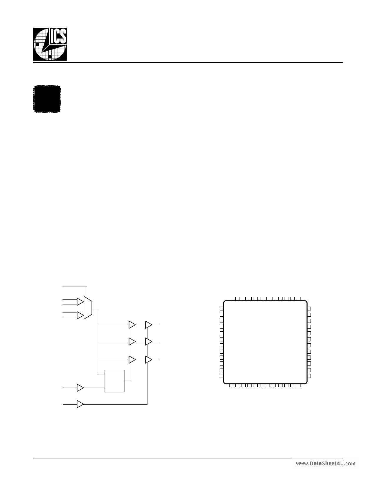
BLOCK DIAGRAM
CLK_SEL
CLK0
nCLK0
CLK1
nCLK1
1
0
CLK_EN
OE
LE
Q
nD
PIN ASSIGNMENT
Q0 - Q7
Q8 - Q15
Q16 - Q23
Q16
Q17
VDDO
GND
Q18
Q19
Q20
Q21
VDDO
GND
Q22
Q23
48 47 46 45 44 43 42 41 40 39 38 37
1 36
2 35
3 34
4 33
5 32
6
7
ICS8344-01
31
30
8 29
9 28
10 27
11 26
12 25
13 14 15 16 17 18 19 20 21 22 23 24
Q7
Q6
VDDO
GND
Q5
Q4
Q3
Q2
VDDO
GND
Q1
Q0
48-Lead LQFP
7mm x 7mm x 1.4mm
Y Package
Top View
8344AY-01
www.icst.com/products/hiperclocks.html
1
REV. B AUGUST 6, 2001
1 page 
Integrated
Circuit
Systems, Inc.
ICS8344-01
LOW SKEW, 1-TO-24
DIFFERENTIAL-TO-LVCMOS FANOUT BUFFER
TABLE 4D. POWER SUPPLY DC CHARACTERISTICS, VDD = 3.3V±5%, VDDO = 2.5V±5%, TA = 0°C TO 70°C
Symbol Parameter
Test Conditions
Minimum Typical
VDD
VDDO
IDD
Positive Supply Voltage
Output Supply Voltage
Quiescent Power Supply Current
3.135
2.375
3.3
2.5
Maximum
3.465
2.625
95
Units
V
V
mA
www.DataSheeTt4AUB.LcEom4E. LVCMOS DC CHARACTERISTICS, VDDI = VDD = 3.3V±5%, VDDO = 2.5V±5%, TA = 0°C TO 70°C
Symbol Parameter
Test Conditions
Minimum Typical
VIH
Input High Voltage
CLK_SEL, CLK_EN,
OE
VIL
Input Low Voltage
CLK_SEL, CLK_EN,
OE
2
-0.3
CLK_EN, OE
IIH
Input High Current
CLK_SEL
CLK_EN, OE
IIL
Input Low Current
CLK_SEL
VOH Output High Voltage
VOL Output Low Voltage
V = V = 3.465V
DD IN
VDD = VIN = 3.465V
VDD = 3.465, VIN = 0V
VDD = 3.465, VIN = 0V
VDD = 3.135V
VDDO = 2.375V
IOH = -27mA
VDD = 3.135V
VDDO = 2.375V
I = 27mA
OL
-150
-5
1.9
Maximum
3.8
0.8
5
150
0.4
Units
V
V
µA
µA
µA
µA
V
V
TABLE 4F. DIFFERENTIAL DC CHARACTERISTICS, VDD = 3.3V±5%, VDDO = 2.5V±5%, TA = 0°C TO 70°C
Symbol Parameter
Test Conditions
Minimum Typical Maximum Units
nCLK0, nCLK1
IIH
Input High Current
CLK0, CLK1
nCLK0, nCLK1
IIL Input Low Current
CLK0, CLK1
VPP Peak-to-Peak Input Voltage
V = V = 3.465V
DD IN
VDD = VIN = 3.465V
VDD = 3.465V,
VIN = 0V
VDD = 3.465V,
VIN = 0V
-150
-5
0.3
5
150
1.3
VCMR
Common Mode Input Voltage; NOTE 1, 2
0.9 2
NOTE 1: For single ended applications, the maximum input voltage for CLK0, nCLK0 and CLK1, nCLK1 is VDD + 0.3V.
NOTE 2: Common mode voltage is defined as VIH.
µA
µA
µA
µA
V
V
8344AY-01
www.icst.com/products/hiperclocks.html
5
REV. B AUGUST 6, 2001
5 Page 
Integrated
Circuit
Systems, Inc.
ICS8344-01
LOW SKEW, 1-TO-24
DIFFERENTIAL-TO-LVCMOS FANOUT BUFFER
APPLICATION INFORMATION
WIRING THE DIFFERENTIAL INPUT TO ACCEPT SINGLE ENDED LEVELS
www.DataSheeFt4igUu.croem8
shows
how
the
differential
input
can
be
wired
to
accept
single
ended
levels.
The
reference
voltage
V_REF
~
V /2
DD
is
generated by the bias resistors R1, R2 and C1. This bias circuit should be located as close as possible to the input pin. The ratio of
R1 and R2 might need to be adjusted to position the V_REF in the center of the input voltage swing. For example, if the input clock
swing is only 2.5V and V = 3.3V, V_REF should be 1.25V and R2/R1 = 0.609.
DD
CLK_IN
C1
0.1uF
VDD
R1
1K
+
V_REF
-
R2
1K
FIGURE 8 - SINGLE ENDED SIGNAL DRIVING DIFFERENTIAL INPUT
8344AY-01
www.icst.com/products/hiperclocks.html
11
REV. B AUGUST 6, 2001
11 Page | ||
| Páginas | Total 16 Páginas | |
| PDF Descargar | [ Datasheet ICS8344-01.PDF ] | |
Hoja de datos destacado
| Número de pieza | Descripción | Fabricantes |
| ICS8344-01 | 1-TO-24 DIFFERENTIAL-TO-LVCMOS FANOUT BUFFER | Integrated Circuit Systems |
| Número de pieza | Descripción | Fabricantes |
| SLA6805M | High Voltage 3 phase Motor Driver IC. |
Sanken |
| SDC1742 | 12- and 14-Bit Hybrid Synchro / Resolver-to-Digital Converters. |
Analog Devices |
|
DataSheet.es es una pagina web que funciona como un repositorio de manuales o hoja de datos de muchos de los productos más populares, |
| DataSheet.es | 2020 | Privacy Policy | Contacto | Buscar |