|
|
|
PDF LH5496H Data sheet ( Hoja de datos )
| Número de pieza | LH5496H | |
| Descripción | CMOS 512 x 9 FIFO | |
| Fabricantes | Sharp Electrionic Components | |
| Logotipo | ||
Hay una vista previa y un enlace de descarga de LH5496H (archivo pdf) en la parte inferior de esta página. Total 16 Páginas | ||
|
No Preview Available !
LH5496/96H
CMOS 512 × 9 FIFO
FEATURES
• Fast Access Times:
15 */20/25/35/50/65/80 ns
• Full CMOS Dual Port Memory Array
• Fully Asynchronous Read and Write
• Expandable-in Width and Depth
• Full, Half-Full, and Empty Status Flags
• Read Retransmit Capability
• TTL Compatible I/O
• Packages:
28-Pin, 300-mil PDIP
28-Pin, 600-mil PDIP
32-Pin PLCC
• Pin and Functionally Compatible with IDT7201
FUNCTIONAL DESCRIPTION
The LH5496/96H are dual port memories with internal
addressing to implement a First-In, First-Out algorithm.
Through an advanced dual port architecture, they provide
fully asynchronous read/write operation. Empty, Full, and
Half-Full status flags are provided to prevent data over-
flow and underflow. In addition, internal logic provides for
unlimited expansion in both word size and depth.
Read and write operations automatically access se-
quential locations in memory in that data is read out in the
same order that it was written, that is on a First-In,
First-Out basis. Since the address sequence is internally
predefined, no external address information is required
for the operation of this device. A ninth data bit is provided
for parity or control information often needed in commu-
nication applications.
Empty, Full, and Half-Full status flags monitor the
extent to which data has been written into the FIFO, and
prevent improper operations (i.e., Read if the FIFO is
empty, or Write if the FIFO is full). A retransmit feature
resets the Read address pointer to its initial position,
thereby allowing repetitive readout of the same data.
Expansion In and Expansion Out pins implement an
expansion scheme that allows individual FIFOs to be
cascaded to greater depth without incurring additional
latency (bubblethrough) delays.
* LH5496 only.
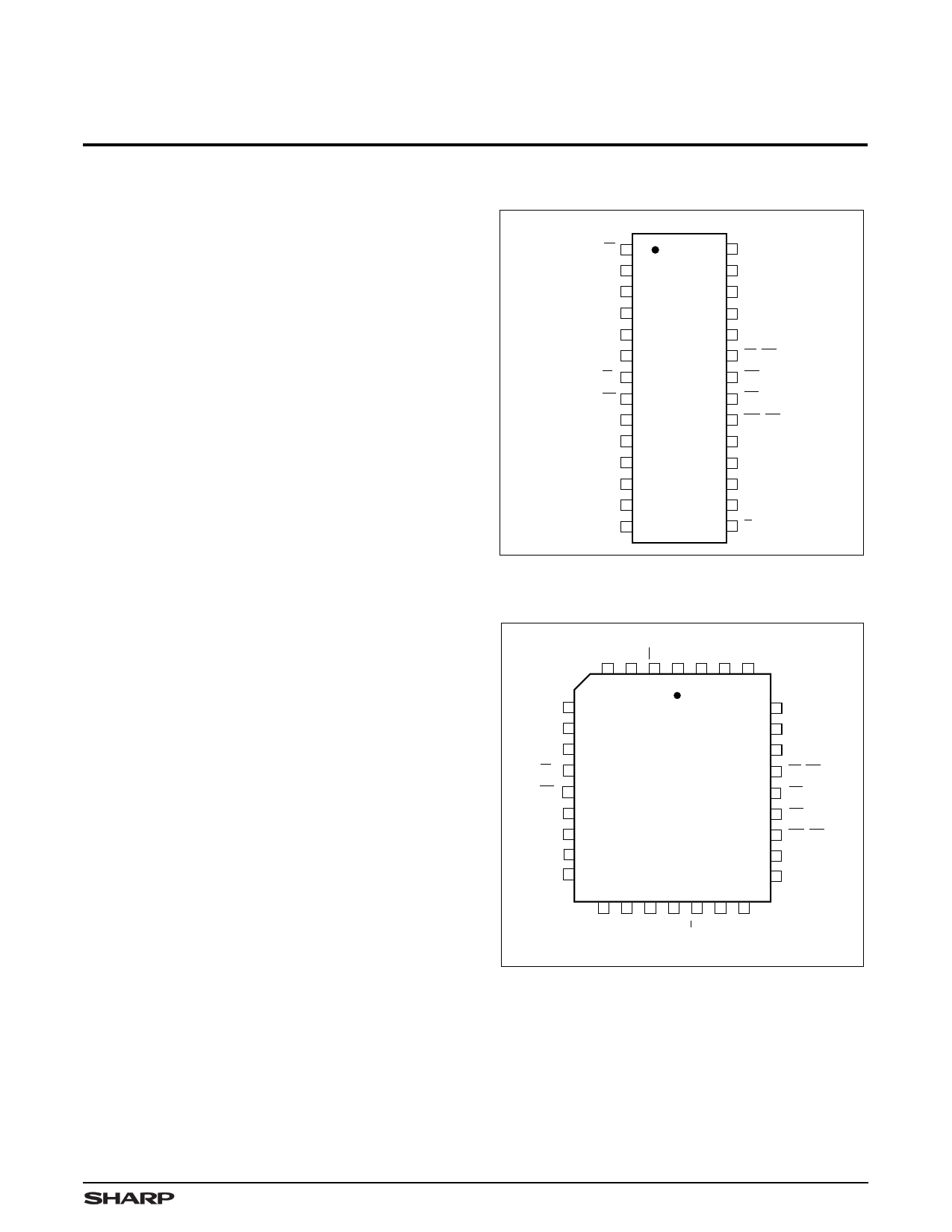
PIN CONNECTIONS
28-PIN PDIP
W
D8
D3
D2
D1
D0
XI
FF
Q0
Q1
Q2
Q3
Q8
VSS
1
2
3
4
5
6
7
8
9
10
11
12
13
14
TOP VIEW
28 VCC
27 D4
26 D5
25 D6
24 D7
23 FL/RT
22 RS
21 EF
20 XO/HF
19 Q7
18 Q6
17 Q5
16 Q4
15 R
5496-1D
Figure 1. Pin Connections for PDIP Packages
32-PIN PLCC
TOP VIEW
4 3 2 1 32 31 30
D2 5
D1 6
D0 7
XI 8
29 D6
28 D7
27 NC
26 FL/RT
FF 9
25 RS
Q0 10
24 EF
Q1 11
23 XO/HF
NC 12
22 Q7
Q2 13
21 Q6
14 15 16 17 18 19 20
5496-2D
Figure 2. Pin Connections for PLCC Package
1
1 page 
CMOS 512 × 9 FIFO
LH5496/96H
AC ELECTRICAL CHARACTERISTICS 1 (Over Operating Range)
SYMBOL
PARAMETER
tA = 15 ns 2 tA = 20 ns tA = 25 ns tA = 35 ns tA = 50 ns tA = 65 ns tA = 80 ns
MIN MAX MIN MAX MIN MAX MIN MAX MIN MAX MIN MAX MIN MAX UNIT
READ CYCLE TIMING
tRC
tA
tRR
tRPW
tRLZ
tWLZ
Read Cycle Time
Access Time
Read Recover Time
Read Pulse Width 3
Data Bus Active from Read LOW 4
Data Bus Active from Write
HIGH 4,5
25
–
10
15
5
10
– 30 – 35 – 45 – 65 – 80 – 100 –
15 – 20 – 25 – 35 – 50 – 65 – 80
– 10 – 10 – 10 – 15 – 15 – 15 –
– 20 – 25 – 35 – 50 – 65 – 80 –
– 5 – 5 – 5 – 5 – 5 – 10 –
– 10 – 10 – 10 – 10 – 10 – 20 –
ns
ns
ns
ns
ns
ns
tDV Data Valid from Read Pulse HIGH 5 – 5 – 5 – 5 – 5 – 5 – 5 – ns
tRHZ
Data Bus High-Z from Read
HIGH 4
– 15 – 15 – 15 – 15 – 20 – 30 – 30 ns
WRITE CYCLE TIMING
tWC
tWPW
Write Cycle Time
Write Pulse Width 3
25 – 30 – 35 – 45 – 65 – 80 – 100 – ns
15 – 20 – 25 – 35 – 50 – 65 – 80 – ns
tWR Write Recovery Time
10 – 10 – 10 – 10 – 15 – 15 – 15 – ns
tDS Data Setup Time
tDH Data Hold Time
10 – 10 – 10 – 15 – 20 – 20 – 20 – ns
0 – 0 – 0 – 0 – 0 – 5 – 5 – ns
RESET TIMING
tRSC Reset Cycle Time
tRS Reset Pulse Width 3
25 – 30 – 35 – 45 – 65 – 80 – 100 – ns
15 – 20 – 25 – 35 – 50 – 65 – 80 – ns
tRSR
tRRSS
tWRSS
Reset Recovery Time
Read HIGH to RS HIGH
Write HIGH to RS HIGH
10 – 10 – 10 – 10 – 15 – 15 – 15 – ns
15 – 20 – 25 – 35 – 50 – 65 – 80 – ns
15 – 20 – 25 – 35 – 50 – 65 – 80 – ns
RETRANSMIT TIMING
tRTC Retransmit Cycle Time
tRT Retransmit Pulse Width 3
tRTR Retransmit Recovery Time
25 – 30 – 35 – 45 – 65 – 80 – 100 – ns
15 – 20 – 25 – 35 – 50 – 65 – 80 – ns
10 – 10 – 10 – 10 – 15 – 15 – 15 – ns
FLAG TIMING
tEFL
tHFH,FFH
Reset LOW to Empty Flag LOW
Reset LOW to Half-Full and Full
Flags HIGH
– 25 – 30 – 35 – 45 – 65 – 80 – 100 ns
– 25 – 30 – 35 – 45 – 65 – 80 – 100 ns
tREF
tRFF
tWEF
tWFF
tWHF
Read LOW to Empty Flag LOW
– 20 – 25 – 25 – 35 – 45 – 60 – 60 ns
Read HIGH to Full Flag HIGH
– 20 – 25 – 25 – 35 – 45 – 60 – 60 ns
Write HIGH to Empty Flag HIGH – 20 – 25 – 25 – 35 – 45 – 60 – 60 ns
Write LOW to Full Flag LOW
– 20 – 25 – 25 – 35 – 45 – 60 – 60 ns
Write LOW to Half-Full Flag LOW – 25 – 30 – 35 – 45 – 65 – 80 – 100 ns
tRHF Read HIGH to Half-Full Flag HIGH – 25 – 30 – 35 – 45 – 65 – 80 – 100 ns
EXPANSION TIMING
tXOL
tXOH
Expansion Out LOW
Expansion Out HIGH
– 18 – 20 – 25 – 35 – 50 – 65 – 80 ns
– 18 – 20 – 25 – 35 – 50 – 65 – 80 ns
tXI Expansion In Pulse Width
15 – 20 – 25 – 35 – 50 – 65 – 80 – ns
tXIR Expansion In Recovery Time 10 – 10 – 10 – 10 – 10 – 10 – 10 – ns
tXIS Expansion in Setup Time
7 – 10 – 10 – 15 – 15 – 15 – 15 – ns
NOTES:
1. LH5496 only.
2. All timing measurements performed at ‘AC Test Condition’ levels.
5
5 Page 
CMOS 512 × 9 FIFO
TIMING DIAGRAMS (cont’d)
tRT
RT
tRTR
R,W
NOTES:
1. tRTC = tRT + tRTR
2. EF, HF and FF may change state during retransmit, but flags will be valid at tRTC.
Figure 14. Retransmit Timing
LH5496/96H
5496-13
WRITE TO LAST
AVAILABLE
LOCATION
W
R
t XOL
t XOH
READ FROM
LAST VALID
LOCATION
t XOL
t XOH
XO
Figure 15. Expansion Out Timing
5496-15
t XI t XIR
XI
t XIS
WRITE TO FIRST
AVAILABLE
W LOCATION
R
t XIS
READ FROM FIRST
VALID
LOCATION
5496-16
Figure 16. Expansion In Timing
11
11 Page | ||
| Páginas | Total 16 Páginas | |
| PDF Descargar | [ Datasheet LH5496H.PDF ] | |
Hoja de datos destacado
| Número de pieza | Descripción | Fabricantes |
| LH5496 | CMOS 512 x 9 FIFO | Sharp Electrionic Components |
| LH5496H | CMOS 512 x 9 FIFO | Sharp Electrionic Components |
| Número de pieza | Descripción | Fabricantes |
| SLA6805M | High Voltage 3 phase Motor Driver IC. |
Sanken |
| SDC1742 | 12- and 14-Bit Hybrid Synchro / Resolver-to-Digital Converters. |
Analog Devices |
|
DataSheet.es es una pagina web que funciona como un repositorio de manuales o hoja de datos de muchos de los productos más populares, |
| DataSheet.es | 2020 | Privacy Policy | Contacto | Buscar |