|
|
|
PDF LH28F040SUTD-Z4 Data sheet ( Hoja de datos )
| Número de pieza | LH28F040SUTD-Z4 | |
| Descripción | 4M (512K bb 8) Flash Memory | |
| Fabricantes | Sharp Electrionic Components | |
| Logotipo | ||
Hay una vista previa y un enlace de descarga de LH28F040SUTD-Z4 (archivo pdf) en la parte inferior de esta página. Total 30 Páginas | ||
|
No Preview Available !
LH28F040SUTD-Z4 4M (512K × 8) Flash Memory
FEATURES
• 512K × 8 Bit Configuration
• 5 V Write/Erase Operation (5V VPP, 3.3 VCC)
– VCC for Write/Erase at as low as 2.9 V
• Min. 2.7 V Read Capability
– 190 ns Maximum Access Time
(VCC = 2.7 V)
• 2 Banks Enable the Simultaneous
Read/Write/Erase Operation
• 32 Independently Lockable Blocks (16K)
• 100,000 Erase Cycles per Block
• Automated Byte Write/Block Erase
– Command User Interface
– Status Register
• System Performance Enhancement
– Erase Suspend for Read
– Two-Byte Write
– Bank Erase
• Data Protection
– Hardware Erase/Write Lockout during
Power Transitions
– Software Erase/Write Lockout
• Independently Lockable for Write/Erase
on Each Block (Lock Block and Protect
Set/Reset)
• 20 µA (Maximum) ICC in CMOS Standby
• State-of-the-Art 0.55 µm ETOX™
Flash Technology
• 40-Pin, 1.2 mm × 10 mm × 20 mm TSOP
(Type I) Package
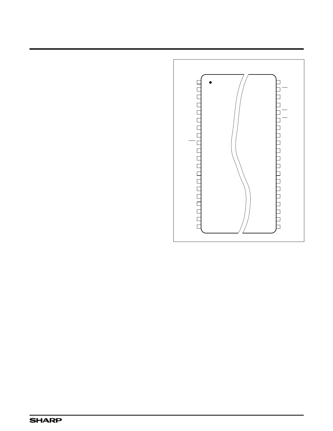
40-PIN TSOP
TOP VIEW
NC1
NC1
A11
A9
A8
A13
A14
A17
WE
VCC
VPP
A16
A15
A12
A7
A6
A5
A4
NC2
NC2
1
2
3
4
5
6
7
8
9
10
11
12
13
14
15
16
17
18
19
20
40 NC
39 OE
38 NC
37 A10
36 BE1
35 BE0
34 DQ7
33 DQ6
32 DQ5
31 DQ4
30 DQ3
29 GND
28 DQ2
27 DQ1
26 DQ0
25 A0
24 A1
23 A2
22 A3
21 NC
28F040SUZ4-1
Figure 1. TSOP Configuration
1
1 page 
4M (512K × 8) Flash Memory
LH28F040SUTD-Z4
The LH28F040SUTD-Z4 incorporates an Automatic
Power Saving (APS) feature which substantially reduces
the active current when the device is in static mode of
operation (addresses not switching).
In APS mode, the typical ICC current is 2 mA at 3.3 V.
A bank reset mode of operation is enabled when
whole BE »0 (or BE »1), WE » and OE » hold low more than 5
µs. In this mode, all operations are aborted, the internal
control circuit is reset and CSR register is cleared.When
the device power up, this bank reset operation must be
executed for each bank to initialize the control circuit. If
BE »X (either BE »0 or BE »1 which is in low state) and or
WE » and or OE » and or goes high, chip reset mode will
be finished. It needs more than 750 ns from one of the
BE »X, WE » or OE » goes high until output data are valid. It
is impossible to reset the whole chip at once, the bank
reset must be executed separately for bank0 and bank1.
A CMOS Standby mode of operation is enabled when
BE X» transitions high with all input control pins at CMOS
levels. In this mode, the device draws an ICC standby
current of 20 µA.
Please do not execute reprogramming 0 for the bit
which has already been programmed 0. Overwrite op-
eration may generate unerasable bit. In case of repro-
gramming 0 to the data which has been programmed 1.
• Program 0 for the bit in which you want to change
data from 1 to 0.
• Program 1 for the bit which has already been pro-
grammed 0.
For example, changing data from 10111101 to
10111100 requires 11111110 programming.
MEMORY MAP
Bank0 (BE0 = Low)
3FFFFH
3C000H
3BFFFH
38000H
37FFFH
34000H
33FFFH
30000H
2FFFFH
2C000H
2BFFFH
28000H
27FFFH
24000H
23FFFH
20000H
1FFFFH
1C000H
1BFFFH
18000H
17FFFH
14000H
13FFFH
10000H
0FFFFH
0C000H
0BFFFH
08000H
07FFFH
04000H
03FFFH
00000H
16KB BLOCK
16KB BLOCK
16KB BLOCK
16KB BLOCK
16KB BLOCK
16KB BLOCK
16KB BLOCK
16KB BLOCK
16KB BLOCK
16KB BLOCK
16KB BLOCK
16KB BLOCK
16KB BLOCK
16KB BLOCK
16KB BLOCK
16KB BLOCK
Bank1 (BE1 = Low)
3FFFFH
15 16KB BLOCK
3C000H
14
3BFFFH
16KB BLOCK
38000H
13
37FFFH
34000H
16KB BLOCK
33FFFH
12
30000H
16KB BLOCK
2FFFFH
11
2C000H
16KB BLOCK
2BFFFH
10
28000H
16KB BLOCK
9
27FFFH
24000H
16KB BLOCK
23FFFH
8
20000H
16KB BLOCK
1FFFFH
7
1C000H
16KB BLOCK
1BFFFH
6
18000H
16KB BLOCK
5
17FFFH
14000H
16KB BLOCK
13FFFH
4
10000H
16KB BLOCK
0FFFFH
3
0C000H
16KB BLOCK
2
0BFFFH
16KB BLOCK
08000H
07FFFH
1
04000H
16KB BLOCK
03FFFH
0 16KB BLOCK
00000H
Figure 3. Memory Map
15
14
13
12
11
10
9
8
7
6
5
4
3
2
1
0
28F040SUZ4-3
5
5 Page 
4M (512K × 8) Flash Memory
LH28F040SUTD-Z4
START
WRITE 20H
WRITE D0H AND
BLOCK ADDRESS
READ COMPATIBLE
STATUS REGISTER
SUSPEND
NO ERASE LOOP
0
CSR.7 =
SUSPEND YES
ERASE
1
CSR FULL STATUS
CHECK IF DESIRED
BUS
OPERATION
COMMAND
COMMENTS
Write
Block Erase D = 20H
A=X
Write
Confirm
D = D0H
A = BA
Read
Q = CSRD
Toggle BE0, BE1 or OE
to update CSRD.
A=X
Standby
Check CSR.7
1 = WSM Ready
0 = WSM Busy
Repeat for subsequent Block Erasures.
CSR Full Status Check can be done after each Block Erase,
or after a sequence of Block Erasures.
Write FFH after the last operation to reset
device to read array mode.
See Command Bus Cycle notes for description of codes.
OPERATION
COMPLETE
CSR FULL STATUS CHECK PROCEDURE
READ CSRD
(see above)
0
CSR.4, 5 =
1
1
CSR.3 =
0
CLEAR CSRD
RETRY/ERROR
RECOVERY
(NOTE)
ERASE
SUCCESSFUL
VPP LOW
DETECT
BUS
OPERATION
COMMAND
COMMENTS
Standby
Check CSR.4, 5
1 = Erase Error
0 = Erase Successful
Both 1 = Command
Sequence Error
Standby
Check CSR.3
1 = VPP Low Detect
0 = VPP OK
CSR.3, 4, 5 should be cleared, if set, before further attempts
are initiated.
NOTE:
If CSR.3 (VPPS) is set to '1', after clearing CSR.3/4/5,
1. Issue Reset WP command.
2. Retry Single Block Erase command.
3. Set WP command is issued, if necessary.
If CSR.3 (VPPS) is set to '0', after clearing CSR.3/4/5,
1. Retry Single Block Erase command.
Where power off or chip reset during erase operation,
1. Clear CSR.3/4/5 and issue Reset WP command,
2. Retry Single Block Erase command.
3. Set WP command is issued, if necessary.
Figure 5. Block Erase with Compatible Status Register
28F040SUZ4-5
11
11 Page | ||
| Páginas | Total 30 Páginas | |
| PDF Descargar | [ Datasheet LH28F040SUTD-Z4.PDF ] | |
Hoja de datos destacado
| Número de pieza | Descripción | Fabricantes |
| LH28F040SUTD-Z4 | 4M (512K bb 8) Flash Memory | Sharp Electrionic Components |
| Número de pieza | Descripción | Fabricantes |
| SLA6805M | High Voltage 3 phase Motor Driver IC. |
Sanken |
| SDC1742 | 12- and 14-Bit Hybrid Synchro / Resolver-to-Digital Converters. |
Analog Devices |
|
DataSheet.es es una pagina web que funciona como un repositorio de manuales o hoja de datos de muchos de los productos más populares, |
| DataSheet.es | 2020 | Privacy Policy | Contacto | Buscar |