|
|
|
PDF SC4905B Data sheet ( Hoja de datos )
| Número de pieza | SC4905B | |
| Descripción | HIGH PERFORMANCE VOLTAGE MODE PWM CONTROLLER | |
| Fabricantes | Semtech Corporation | |
| Logotipo | ||
Hay una vista previa y un enlace de descarga de SC4905B (archivo pdf) en la parte inferior de esta página. Total 20 Páginas | ||
|
No Preview Available !
POWER MANAGEMENT
Description
The SC4905A/B is a 10 pin BICMOS primary side voltage
mode controller for use in Isolated DC-DC and off-line
switching power supplies. It is a highly integrated solution,
requiring few external components. The device features a
high speed oscillator with integrated feed forward
compensation, accurately programmable maximum duty
cycle, voltage mode of operation, line voltage monitoring,
supply UVLO, low start up current, low voltage current limit
www.DataSthhreeets4hUo.clodmand user accessible reference.
The SC4905A/B device operates at a fixed frequency,
highly desirable for Telecom applications. Features a
separate SYNC pin which simplifies synchronization to
an external clock. Feeding the oscillator of one device to
the SYNC of another forces biphase operation (180
degrees apart) which reduces input ripple and filter size.
The SC4905A has a turn-on threshold of 4.5V and the
SC4905B has a turn-on threshold of about 12 volts.
These devices are available in the 10 lead MSOP package.
SC4905A/B
High Performance Voltage Mode
PWM Controller
PRELIMINARY
Features
K Operation to 1MHz
K Accurate programmable maximum duty cycle
K Integrated oscillator/voltage feed forward
compensation
K Line voltage monitoring
K External frequency synchronization
K Bi-phase mode of operation for ripple reduction
K Under 100µA start-up current
K Accessible reference voltage
K VDD undervoltage lockout
K -40°C to 105°C operating temperature
K 10 lead MSOP package
Applications
K Telecom equipment and power supplies
K Networking power supplies
K Power over LAN applications
K Industrial power supplies
K Isolated power supplies
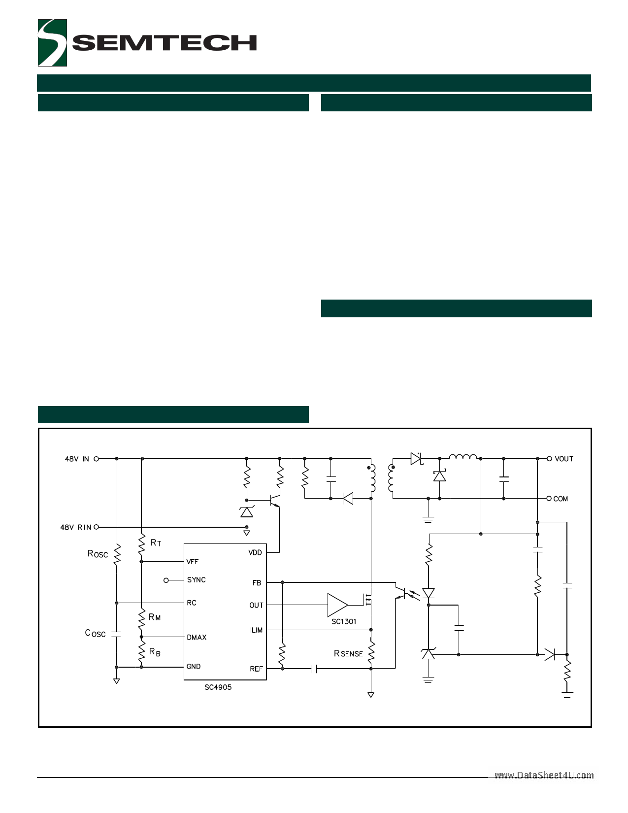
Typical Application Circuit
Revision 4, April 2002
1
www.semtech.com
1 page 
SC4905A/B
POWER MANAGEMENT
Pin Descriptions
VDD: The supply input for the device. Once VDD has ex-
ceeded the UVLO limit, the internal reference, oscillator,
drivers and logic are powered up. This pin should be by-
passed with a low ESR capacitance right at the IC pin to
minimize noise problems, and to ensure proper opera-
tion.
FB: Input to the PWM comparator with an offset voltage
of 700mV. The feedback analog signal from the output
of an error amplifier or an Optoisolator will be connected
www.DatatSoheteht4isU.pcoinm to provide regulation.
VFF: The VFF pin provides the controller with a voltage
proportional to the power supply input voltage to achieve
feed-forward function. RM plus RB in conjunction with RT
will set the Vff level (see page 1 circuit).
VFF =
(RB + RM)
(RT + RB + RM)
DMAX: Programmable duty cycle is achieved via resis-
tive divider from the VFF. The duty cycle percentage is
set by the ratio of the divider RM, and RB (see page 1
circuit) from the VFF signal. When RM is shorted, maxi-
mum duty cycle of 100% is achieved. RM plus RB in con-
junction with RT will also be used as the divider to set the
Vff level.
PRELIMINARY
Where VFF is the voltage at the VFF pin at a given Vin,
frequency is in Hertz, resistance in ohms, and capaci-
tance in farads.
The recommended range if timing resistors is between
10 kohm and 500kohm and range of timing capacitors
is between 100pF and 1000pF. Timing resistors less
than 10 kohm should be avoided.
Refer to layout guide lines on page 16 to achieve best
results.
SYNC: SYNC is a positive edge triggered input with a
threshold precisely set to
0.5*VFF
In the Bi-Phase operation mode SYNC pins should be con-
nected to the Cosc (Timing Capacitors) of the other con-
troller. This will force a 180° out of phase operation.
(see page9).
In a single controller operation, SYNC could be grounded
or connected to an external synchronization clock with Fre-
quency higher than the on board oscillator Frequency (see
page 2).
ILIM: Current sense input is provided via the ILIM pin.
The current sense input from a sense resistor provides a
pulse by pulse current limit by terminating the PWM pulse
when the input is above 200mV.
DutyCycle% = VDMAX
VFF
RC: The oscillator programming pin. The oscillator should
be referenced to Vin to achieve the line feed forward func-
tion. Only two components are required to program the
oscillator, a resistor ROSC (tied to the Vin and RC), and a
capacitor COSC (tied to the RC and GND). Since the peak
oscillator voltage is VFF, constant frequency operation is
maintained over the full power supply. When the DMAX
pin is shorted to the VFF pin, the oscillator can run at the
largest duty cycle possible.
Following formula can be used for a close approximation
of the Oscillator Frequency.
GND: Device power and analog ground. Careful atten-
tion should be paid to the layout of the ground planes
(see page 12).
OUT: The output is intended to drive an external FET driver
or other high impedance circuit. The output voltage swings
from GND to Vref with a typical output impedance of 500Ω.
REF: The REF pin provides a 4 or 5V user accessible
voltage reference. This pin should be decoupled with a
1µF capacitor.
FOSC
≅
(ROSC
Vin−
• COSC
VFF
2
• VFF•1.05)
2002 Semtech Corp.
5
www.semtech.com
5 Page 
POWER MANAGEMENT
Application Information (Cont.)
START UP SEQUENCE
Initially during the power up, the SC4905 is in the under
voltage lock out condition. As the VDD supply exceeds
the UVLO limit of the SC4905 and the VFF pin exceeds
the line under voltage lock out of about 1.2V, the inter-
nal reference, oscillator, and logic circuitry are powered
up.
www.DataTShheeetO4UU.Tcodmriver is not enabled until the line under voltage
lock out limit is reached. At that point, once the FB pin
has reached above 600mV, the output driver is enabled.
As the output voltage starts to increase, the error signal
from the error amplifier starts to decrease. If isolation is
required, the error amplifier output can drive the LED of
the opto isolator. The output of the opto is connected in
a common emitter configuration with a pull up resistor to
a reference voltage connected to the FB pin of the
SC4905. The voltage level at the FB pin provides the duty
cycle necessary to achieve regulation.
SC4905A/B
PRELIMINARY
2002 Semtech Corp.
11
www.semtech.com
11 Page | ||
| Páginas | Total 20 Páginas | |
| PDF Descargar | [ Datasheet SC4905B.PDF ] | |
Hoja de datos destacado
| Número de pieza | Descripción | Fabricantes |
| SC4905A | HIGH PERFORMANCE VOLTAGE MODE PWM CONTROLLER | Semtech Corporation |
| SC4905B | HIGH PERFORMANCE VOLTAGE MODE PWM CONTROLLER | Semtech Corporation |
| Número de pieza | Descripción | Fabricantes |
| SLA6805M | High Voltage 3 phase Motor Driver IC. |
Sanken |
| SDC1742 | 12- and 14-Bit Hybrid Synchro / Resolver-to-Digital Converters. |
Analog Devices |
|
DataSheet.es es una pagina web que funciona como un repositorio de manuales o hoja de datos de muchos de los productos más populares, |
| DataSheet.es | 2020 | Privacy Policy | Contacto | Buscar |