|
|
|
PDF WCSN0436V1P Data sheet ( Hoja de datos )
| Número de pieza | WCSN0436V1P | |
| Descripción | 128Kx36 Pipelined SRAM | |
| Fabricantes | Weida Semiconductor | |
| Logotipo | ||
Hay una vista previa y un enlace de descarga de WCSN0436V1P (archivo pdf) en la parte inferior de esta página. Total 14 Páginas | ||
|
No Preview Available !
Y7C1350B
WCSN0436V1P
Features
128Kx36 Pipelined SRAM with NoBL™ Architecture
Functional Description
• Pin compatible and functionally equivalent to ZBT™
devices IDT71V546, MT55L128L36P, and MCM63Z736
• Supports 166-MHz bus operations with zero wait states
— Data is transferred on every clock
• Internally self-timed output buffer control to eliminate
the need to use OE
• Fully registered (inputs and outputs) for pipelined
operation
www.DataShe•etB4Uy.tceomWrite capability
• 128K x 36 common I/O architecture
• Single 3.3V power supply
• Fast clock-to-output times
— 3.5 ns (for 166-MHz device)
— 3.8 ns (for 150-MHz device)
— 4.0 ns (for 143-MHz device)
— 4.2 ns (for 133-MHz device)
— 5.0 ns (for 100-MHz device)
— 7.0 ns (for 80-MHz device)
• Clock Enable (CEN) pin to suspend operation
• Synchronous self-timed writes
• Asynchronous output enable
• JEDEC-standard 100 TQFP package
• Burst Capability—linear or interleaved burst order
• Low standby power (17.325 mW max.)
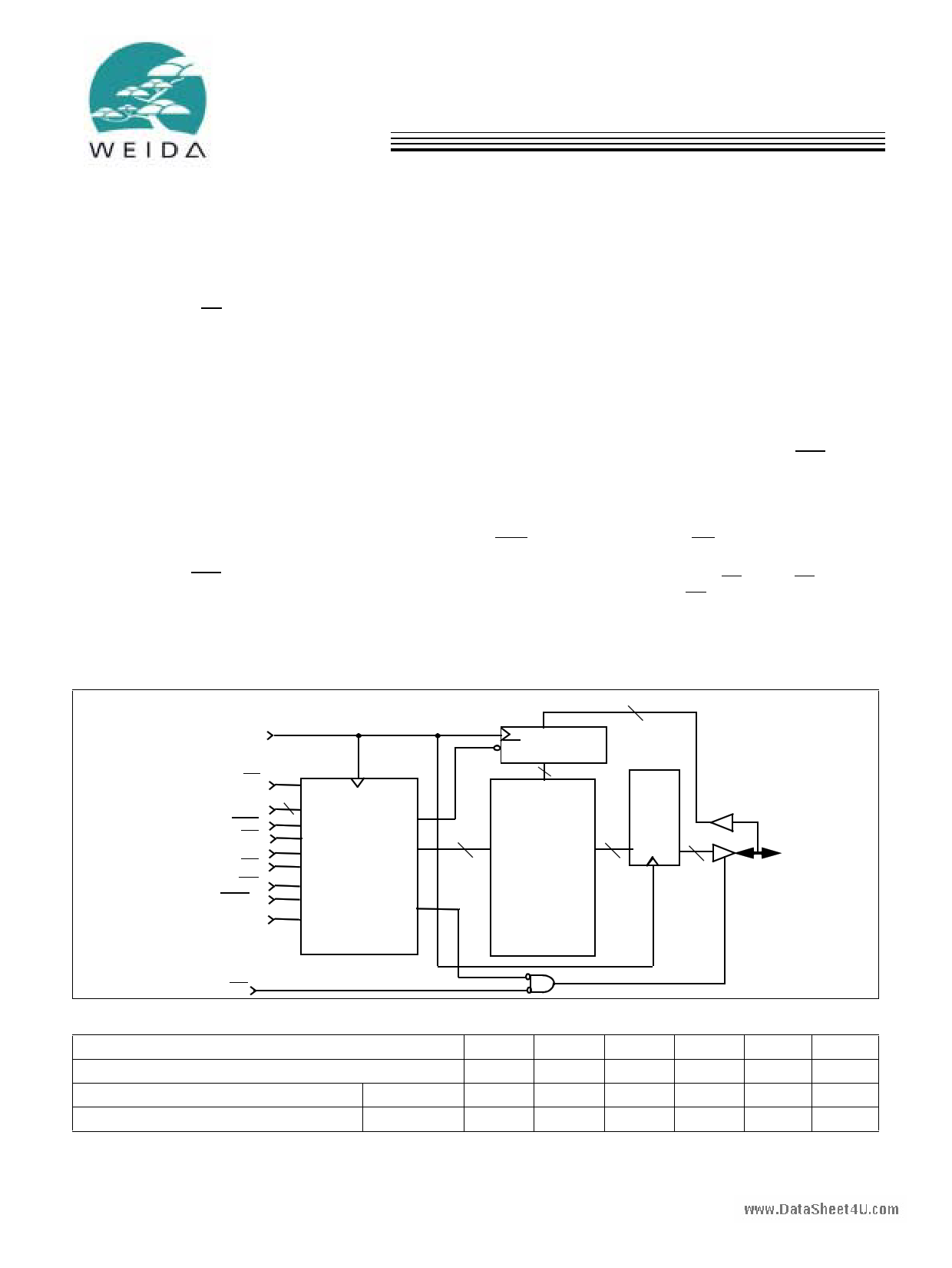
Logic Block Diagram
CLK
ADV/LD
A[16:0] 17
CEN
CE1
CE2
CE3
WE
BWS[3:0]
MODE
CONTROL
and WRITE
LOGIC
17
The WCSN0436V1P is a 3.3V, 128K by 36 synchronous-pipe-
lined Burst SRAM designed specifically to support unlimited
true back-to-back Read/Write operations without the insertion
of wait states. The WCSN0436V1P is equipped with the ad-
vanced No Bus Latency™ (NoBL™) logic required to enable
consecutive Read/Write operations with data being trans-
ferred on every clock cycle. This feature dramatically improves
the throughput of the SRAM, especially in systems that require
frequent Write/Read transitions.The WCSN0436V1P is
pin/functionally compatible to ZBT SRAMsIDT71V546,
MT55L128L36P, and MCM63Z736.
All synchronous inputs pass through input registers controlled
by the rising edge of the clock. All data outputs pass through
output registers controlled by the rising edge of the clock. The
clock input is qualified by the Clock Enable (CEN) signal,
which when deasserted suspends operation and extends the
previous clock cycle. Maximum access delay from the clock
rise is 3.5 ns (166-MHz device).
Write operations are controlled by the four Byte Write Select
(BWS[3:0]) and a Write Enable (WE) input. All writes are con-
ducted with on-chip synchronous self-timed write circuitry.
Three synchronous Chip Enables (CE1, CE2, CE3) and an
asynchronous Output Enable (OE) provide for easy bank se-
lection and output three-state control. In order to avoid bus
contention, the output drivers are synchronously three-stated
during the data portion of a write sequence.
CE
DaDta-In
Q
REG.
36
36
128Kx36
MEMORY
ARRAY
36
36
DQ[31:0]
DP[3:0]
OE
Selection Guide
.
Maximum Access Time (ns)
Maximum Operating Current (mA)
Maximum CMOS Standby Current (mA)
.
.
Commercial
Commercial
-166
3.5
400
5
-150
3.8
375
5
-143
4.0
350
5
-133
4.2
300
5
-100
5.0
250
5
-80
7.0
200
5
Document#: 38-05246
Revised Jan 06,2002
1 page 
WCSN0436V1P
and DP[3:0] are automatically three-stated during the data por-
tion of a write cycle, regardless of the state of OE.
Burst Write Accesses
The WCSN0436V1p has an on-chip burst counter that allows
the user the ability to supply a single address and conduct up
to four WRITE operations without reasserting the address in-
puts. ADV/LD must be driven LOW in order to load the initial
address, as described in the Single Write Access section
above. When ADV/LD is driven HIGH on the subsequent clock
rise, the chip enables (CE1, CE2, and CE3) and WE inputs are
ignored and the burst counter is incremented. The correct
BWS[3:0] inputs must be driven in each cycle of the burst write
in order to write the correct bytes of data.
www.DataSheet4U.com
Interleaved Burst Sequence
First
Address
Ax+1, Ax
00
01
10
11
Second
Address
Ax+1, Ax
01
00
11
10
Third
Address
Ax+1, Ax
10
11
00
01
Fourth
Address
Ax+1, Ax
11
10
01
00
Linear Burst Sequence
First
Address
Ax+1, Ax
00
01
10
11
Second
Address
Ax+1, Ax
01
10
11
00
Third
Address
Ax+1, Ax
10
11
00
01
Fourth
Address
Ax+1, Ax
11
00
01
10
Cycle Description Truth Table[1, 2, 3, 4, 5, 6]
Operation
Address
ADV/
Used
CE CEN LD/
WE BWSx CLK
Comments
Deselected
External
1
0
L
X
X L-H
I/Os three-state following next rec-
ognized clock.
Suspend
-
X
1
X
X
X L-H
Clock ignored, all operations sus-
pended.
Begin Read
External
00
0
1
X L-H Address latched.
Begin Write
External
00
0
0 Valid L-H Address latched, data presented
two valid clocks later.
Burst Read
Operation
Internal
X0
1
X
X L-H
Burst Read operation. Previous ac-
cess was a Read operation. Ad-
dresses incremented internally in
conjunction with the state of
MODE.
Burst Write
Operation
Internal
X 0 1 X Valid L-H Burst Write operation. Previous ac-
cess was a Write operation. Ad-
dresses incremented internally in
conjunction with the state of
MODE. Bytes written are deter-
mined by BWS[3:0].
Notes:
1. X=”Don't Care”, 1=Logic HIGH, 0=Logic LOW, CE stands for ALL Chip Enables active. BWSx = 0 signifies at least one Byte Write Select is active, BWSx =
Valid signifies that the desired byte write selects are asserted, see Write Cycle Description table for details.
2. Write is defined by WE and BWS[3:0]. See Write Cycle Description table for details.
3. The DQ and DP pins are controlled by the current cycle and the OE signal.
4. CEN=1 inserts wait states.
5. Device will power-up deselected and the I/Os in a three-state condition, regardless of OE.
6. OE assumed LOW.
Document #: 38-05246 Rev. **
Page 5 of 14
5 Page 
Switching Waveforms (continued)
Burst Sequences
WCSN0436V1P
CLK
tALS
www.DataSheet4AUD.cVom/LD
tALH
ADDRESS RA1
tCH tCL
tCYC
tAS tAH
WA2
RA3
WE
tWS tWH
BWS[3:0]
tWS tWH
tCES tCEH
CE
Data-
In/Out
tCLZ
Device
originally
deselected
tDOH
Q1 Q1+1
Out Out
tCO tCO
tCHZ
tDH
Q1+2 Q1+3
Out Out
D2 D2+1
In In
tDS
D2+2
In
tCLZ
D2+3
In
Q3
Out
The combination of WE & BWS[3:0] define a write cycle (see Write Cycle Description table).
CE is the combination of CE1, CE2, and CE3. All chip enables need to be active in order to select
the device. Any chip enable can deselect the device. RAx stands for Read Address X, WA stands for
Write Address X, Dx stands for Data-in for location X, Qx stands for Data-out for location X. CEN held
LOW. During burst writes, byte writes can be conducted by asserting the appropriate BWS[3:0] input signals.
Burst order determined by the state of the MODE input. CEN held LOW. OE held LOW.
= DON’T CARE = UNDEFINED
Document #: 38-05246 Rev. **
Page 11 of 14
11 Page | ||
| Páginas | Total 14 Páginas | |
| PDF Descargar | [ Datasheet WCSN0436V1P.PDF ] | |
Hoja de datos destacado
| Número de pieza | Descripción | Fabricantes |
| WCSN0436V1P | 128Kx36 Pipelined SRAM | Weida Semiconductor |
| Número de pieza | Descripción | Fabricantes |
| SLA6805M | High Voltage 3 phase Motor Driver IC. |
Sanken |
| SDC1742 | 12- and 14-Bit Hybrid Synchro / Resolver-to-Digital Converters. |
Analog Devices |
|
DataSheet.es es una pagina web que funciona como un repositorio de manuales o hoja de datos de muchos de los productos más populares, |
| DataSheet.es | 2020 | Privacy Policy | Contacto | Buscar |