|
|
PDF IDT74LVCH16652 Data sheet ( Hoja de datos )
| Número de pieza | IDT74LVCH16652 | |
| Descripción | 3.3V CMOS 16-BIT BUS TRANSCEIVER AND REGISTER | |
| Fabricantes | Integrated Device Technology | |
| Logotipo |  |
|
Hay una vista previa y un enlace de descarga de IDT74LVCH16652 (archivo pdf) en la parte inferior de esta página. Total 8 Páginas | ||
|
No Preview Available !
IDT74LVCH16652
3.3V CMOS 16-BIT BUS TRANSCEIVER AND REGISTER
INDUSTRIALTEMPERATURERANGE
3.3V CMOS 16-BIT BUS
TRANSCEIVER AND REGISTER
WITH 3-STATE OUTPUTS,
5V TOLERANT I/O, BUS-HOLD
IDT74LVCH16652
FEATURES:
• Typical tSK(o) (Output Skew) < 250ps
• ESD > 2000V per MIL-STD-883, Method 3015; > 200V using
machine model (C = 200pF, R = 0)
• VCC = 3.3V ± 0.3V, Normal Range
• VCC = 2.7V to 3.6V, Extended Range
• CMOS power levels (0.4µ W typ. static)
www.Data•ShAelelt4inUp.cuotsm, outputs, and I/O are 5V tolerant
• Supports hot insertion
• Available in SSOP and TSSOP packages
DRIVE FEATURES:
• High Output Drivers: ±24mA
• Reduced system switching noise
APPLICATIONS:
• 5V and 3.3V mixed voltage systems
• Data communication and telecommunication systems
DESCRIPTION:
This 16-bit transceiver and register is built using advanced dual metal CMOS
technology. This high-speed, low power device is organized as twoindependent
8-bit bus transceivers with 3-state D-type registers. The control circuitry is
organized for multiplexed transmission of data between A bus and B bus either
directly or from the internal storage registers. Each 8-bit transceiver/register
features complementary Output Enable (OEAB and OEBA) inputs to control the
transciever functions and Select lines (SAB and SBA) to select either real-time
data or stored data. Separate clock inputsare provided for A and B port
registers. Data on the A or B data bus, or both,can be stored in the internal
registers by the low-to-high transitions at theappropriate clock pins. Flow-
through organization of signal pins simplifieslayout. All inputs are designed with
hysteresis for improved noise margin.
The LVCH16652A has been designed with a ±24mA output driver. This
driver is capable of driving a moderate to heavy load while maintaining speed
performance.
The LVCH16652A has “bus-hold” which retains the inputs’ last state
whenever the input bus goes to a high impedance. This prevents floating inputs
and eliminates the need for pull-up/down resistors.
FUNCTIONAL BLOCK DIAGRAM
1OEBA 56
1OEAB 1
1CLKBA 55
1SBA 54
1CLKAB 2
1SAB 3
1A1 5
A REG
D
C
B REG
D
C
2OEBA 29
2OEAB 28
2CLKBA 30
2SBA 31
2CLKAB 27
2SAB 26
52 1B1
2A1 15
A REG
D
C
B REG
D
C
42 2B1
TO 7 OTHER CHANNELS
The IDT logo is a registered trademark of Integrated Device Technology, Inc.
INDUSTRIAL TEMPERATURE RANGE
© 2004 Integrated Device Technology, Inc.
1
TO 7 OTHER CHANNELS
JANUARY 2004
DSC-4689/3
1 page 
IDT74LVCH16652
3.3V CMOS 16-BIT BUS TRANSCEIVER AND REGISTER
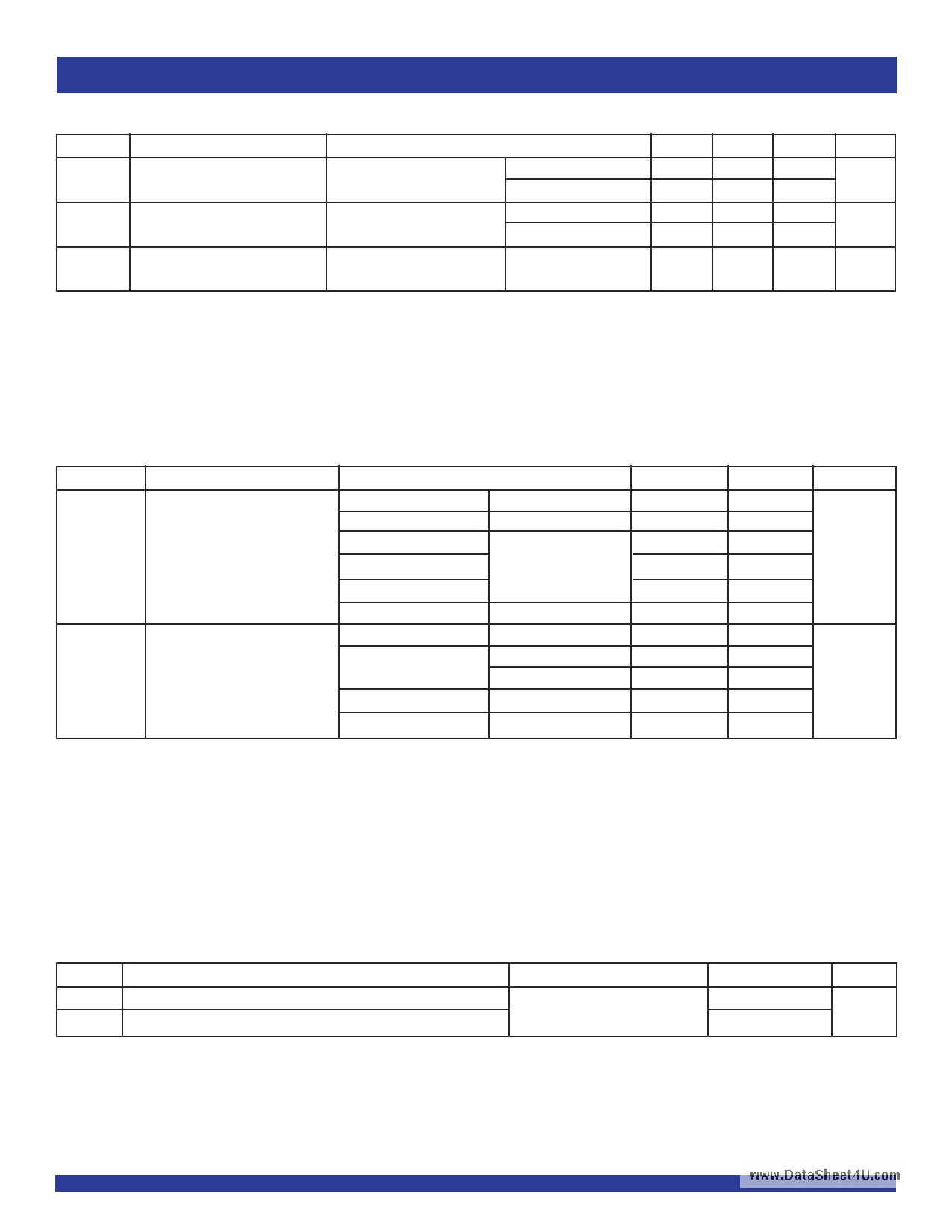
BUS-HOLD CHARACTERISTICS
Symbol Parameter(1)
IBHH Bus-Hold Input Sustain Current VCC = 3V
IBHL
IBHH Bus-Hold Input Sustain Current VCC = 2.3V
IBHL
IBHHO
Bus-Hold Input Overdrive Current VCC = 3.6V
IBHLO
NOTES:
1. Pins with Bus-Hold are identified in the pin description.
2. Typical values are at VCC = 3.3V, +25°C ambient.
www.DataSheet4U.com
Test Conditions
VI = 2V
VI = 0.8V
VI = 1.7V
VI = 0.7V
VI = 0 to 3.6V
INDUSTRIALTEMPERATURERANGE
Min. Typ.(2) Max. Unit
– 75 —
— µA
75 —
—
——
— µA
——
—
— — ±500 µA
OUTPUT DRIVE CHARACTERISTICS
Symbol
Parameter
Test Conditions(1)
VOH Output HIGH Voltage
VCC = 2.3V to 3.6V
IOH = – 0.1mA
VCC = 2.3V
IOH = – 6mA
VCC = 2.3V
IOH = – 12mA
VCC = 2.7V
VCC = 3V
VCC = 3V
IOH = – 24mA
VOL OutputLOWVoltage
VCC = 2.3V to 3.6V
IOL = 0.1mA
VCC = 2.3V
IOL = 6mA
IOL = 12mA
VCC = 2.7V
IOL = 12mA
VCC = 3V
IOL = 24mA
Min. Max. Unit
VCC – 0.2
—
V
2—
1.7 —
2.2 —
2.4 —
2—
— 0.2 V
— 0.4
— 0.7
— 0.4
— 0.55
NOTE:
1. VIH and VIL must be within the min. or max. range shown in the DC ELECTRICAL CHARACTERISTICS OVER OPERATING RANGE table for the appropriate VCC range.
TA = – 40°C to + 85°C.
OPERATING CHARACTERISTICS, VCC = 3.3V ± 0.3V, TA = 25°C
Symbol
CPD
CPD
Parameter
Power Dissipation Capacitance per Transceiver Outputs enabled
Power Dissipation Capacitance per Transceiver Outputs disabled
Test Conditions
CL = 0pF, f = 10Mhz
Typical
55
12
Unit
pF
5
5 Page | ||
| Páginas | Total 8 Páginas | |
| PDF Descargar | [ Datasheet IDT74LVCH16652.PDF ] | |
Hoja de datos destacado
| Número de pieza | Descripción | Fabricantes |
| IDT74LVCH16652 | 3.3V CMOS 16-BIT BUS TRANSCEIVER AND REGISTER | Integrated Device Technology |
| Número de pieza | Descripción | Fabricantes |
| SLA6805M | High Voltage 3 phase Motor Driver IC. |
Sanken |
| SDC1742 | 12- and 14-Bit Hybrid Synchro / Resolver-to-Digital Converters. |
Analog Devices |
|
DataSheet.es es una pagina web que funciona como un repositorio de manuales o hoja de datos de muchos de los productos más populares, |
| DataSheet.es | 2020 | Privacy Policy | Contacto | Buscar |
