|
|
|
PDF ADUM5230 Data sheet ( Hoja de datos )
| Número de pieza | ADUM5230 | |
| Descripción | Isolated Half-Bridge Driver | |
| Fabricantes | Analog Devices | |
| Logotipo | ||
Hay una vista previa y un enlace de descarga de ADUM5230 (archivo pdf) en la parte inferior de esta página. Total 16 Páginas | ||
|
No Preview Available !
Isolated Half-Bridge Driver
with Integrated High-Side Supply
ADuM5230
FEATURES
Integrated, isolated high-side supply
150 mW of secondary side power
Isolated high-side and low-side outputs
100 mA output source current, 300 mA output sink current
High common-mode transient immunity: >25 kV/μs
High temperature operation: 105°C
www.DataSheeAt4dUju.csotmable power level
Wide body 16-lead SOIC package
Safety and regulatory approvals (pending)
UL recognition: 2500 V rms for 1 minute per UL1577
APPLICATIONS
MOSFET/IGBT gate drive
Plasma display modules
Motor drives
Power supplies
Solar panel inverters
GENERAL DESCRIPTION
The ADuM52301 is an isolated half-bridge gate driver that
employs Analog Devices, Inc., iCoupler® technology to provide
independent and isolated high-side and low-side outputs.
Combining CMOS and microtransformer technologies, this
isolation component contains an integrated dc-to-dc converter
providing an isolated high-side supply. This eliminates the cost,
space, and performance difficulties associated with external
supply configurations such as a bootstrap circuitry. This high-
side isolated supply powers not only the ADuM5230 high-side
output but also any external buffer circuitry used with the
ADuM5230.
In comparison to gate drivers employing high voltage level
translation methodologies, the ADuM5230 offers the benefit
of true, galvanic isolation between the input and each output.
Each output can operate up to ±700 VP relative to the input,
thereby supporting low-side switching to negative voltages.
The differential voltage between the high-side and low-side
may be as high as 700 VP.
1 Protected by U.S. Patents 5,952,849; 6,873,065; 6,903,578; 7,075,329; other
pending patents.
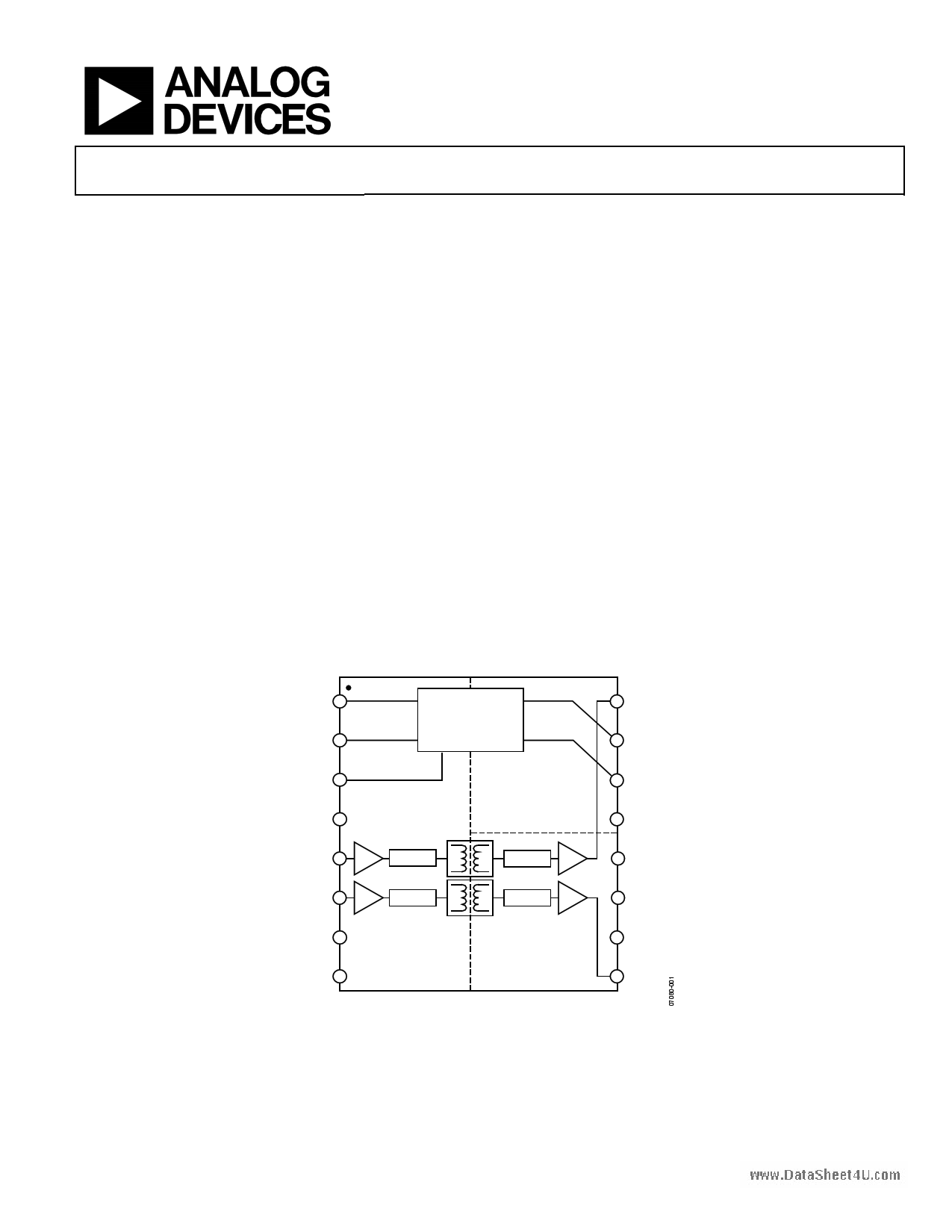
FUNCTIONAL BLOCK DIAGRAM
GND1 1
VDD1 2
VADJ 3
ISOLATED
DC/DC
CONVERTER
GND1 4
VIA 5
╓
╜
VIB 6
╓
╜
ENCODE
ENCODE
DECODE
╓
╜
DECODE
╓
╜
VDD1 7
GND1 8
ADuM5230
NC = NO CONNECT
Figure 1.
16 VOA
15 VISO
14 GNDISO
13 NC
12 NC
11 GNDB
10 VDDB
9 VOB
Rev. 0
Information furnished by Analog Devices is believed to be accurate and reliable. However, no
responsibility is assumed by Analog Devices for its use, nor for any infringements of patents or other
rights of third parties that may result from its use. Specifications subject to change without notice. No
license is granted by implication or otherwise under any patent or patent rights of Analog Devices.
Trademarksandregisteredtrademarksarethepropertyoftheirrespectiveowners.
One Technology Way, P.O. Box 9106, Norwood, MA 02062-9106, U.S.A.
Tel: 781.329.4700
www.analog.com
Fax: 781.461.3113
©2008 Analog Devices, Inc. All rights reserved.
1 page 
ADuM5230
PACKAGE CHARACTERISTICS
Table 2.
Parameter
Resistance (Input-to-Output)1
Capacitance (Input-to-Output)1
Input Capacitance
IC Junction-to-Ambient Thermal Resistance
Symbol Min Typ
RI-O 1012
CI-O 2.0
CI 4.0
θJA 48
Max Unit Test Conditions
Ω
pF f = 1 MHz
pF
°C/W
1 The device is considered a two-terminal device: Pin 1 to Pin 8 are shorted together, and Pin 9 to Pin 16 are shorted together.
REGULATORY INFORMATION
The ADuM5230 will be approved by the organization listed in Table 3.
www.DataSheet4U.com
Table 3.
UL1 (pending)
Recognized under 1577 component recognition program, File E214100
1 In accordance with UL1577, each ADuM5230 is proof-tested by applying an insulation test voltage ≥3000 V rms for 1 sec (current leakage detection limit = 5 μA).
INSULATION AND SAFETY-RELATED SPECIFICATIONS
Table 4.
Parameter
Rated Dielectric Insulation Voltage
Minimum External Air Gap (Clearance)
Symbol
L(I01)
Value
2500
3.5 min
Unit
V rms
mm
Minimum External Tracking (Creepage) L(I02)
3.5 min
mm
Minimum Internal Gap (Internal
Clearance)
Tracking Resistance (Comparative
Tracking Index)
Isolation Group
0.017 min mm
CTI >175 V
IIIa
Conditions
1 minute duration
Measured from input conductors to output conductors,
shortest distance through air
Measured from input conductors to output conductors,
shortest distance path along body
Distance through the insulation
DIN IEC 112/VDE 0303 Part 1
Material Group (DIN VDE 0110, 1/89, Table 1)
600
500
400
300
200
100
0
–40 0 40 80 120 160 200
AMBIENT TEMPERATURE (°C)
Figure 2. Thermal Derating Curve, Dependence of Safety Limiting Values on
Case Temperature, per DIN EN 60747-5-2
RECOMMENDED OPERATING CONDITIONS
Table 5.
Parameter
Operating Temperature (TA)
Input Supply Voltage1 (VDD1)
Channel B Supply Voltage1 (VDDB)
Input Signal Rise and Fall Times
Minimum VDD1 Power-On Slew Rate2 (PSLEW)
Value
−40°C to +105°C
4.5 V to 5.5 V
12 V to 18.5 V
1 ms
400 V/ms
1 All voltages are relative to their respective ground.
2 The ADuM5230 power supply may fail to initialize properly if VDD1 is applied
too slowly.
Rev. 0 | Page 5 of 16
5 Page 
PROPAGATION DELAY-RELATED PARAMETERS
Propagation delay is a parameter that describes the time it takes
a logic signal to propagate through a component. The propagation
delay to a logic low output may differ from the propagation
delay to a logic high.
INPUT (VIx)
OUTPUT (VOx)
tPLH
tPHL
50%
50%
Figure 16. Propagation Delay Parameters
www.DataSheePt4uUls.ecowmidth distortion is the maximum difference between
these two propagation delay values and is an indication of how
accurately the input signal timing is preserved.
Channel-to-channel matching refers to the maximum amount
the propagation delay differs between channels within a single
ADuM5230 component.
DC CORRECTNESS AND MAGNETIC FIELD IMMUNITY
Positive and negative logic transitions at the isolator input
cause narrow (~1 ns) pulses to be sent to the decoder via the
transformer. The decoder is bistable and is, therefore, either set
or reset by the pulses, indicating input logic transitions. In the
absence of logic transitions at the input for more than 1 μs, a
periodic set of refresh pulses indicative of the correct input state
are sent to ensure dc correctness at the output. If the decoder
receives no internal pulses of more than about 5 μs, the input
side is assumed to be unpowered or nonfunctional, in which
case the isolator output is forced to a default state (see Table 9)
by the watchdog timer circuit.
The limitation on the ADuM5230 magnetic field immunity is set
by the condition in which induced voltage in the transformer
receiving coil is sufficiently large to either falsely set or reset the
decoder. The following analysis defines the conditions under
which this may occur.
The pulses at the transformer output have an amplitude greater
than 1.0 V. The decoder has a sensing threshold at about 0.5 V, thus
establishing a 0.5 V margin in which induced voltages can be
tolerated. The voltage induced across the receiving coil is given by
V = (= dβ / dt )∑ πrn 2 ; n = 1, 2, … , N
where:
β is magnetic flux density (gauss).
N is the number of turns in the receiving coil.
rn is the radius of the nth turn in the receiving coil (cm).
Given the geometry of the receiving coil in the ADuM5230 and
an imposed requirement that the induced voltage be at most
50% of the 0.5 V margin at the decoder, a maximum allowable
magnetic field is calculated, as shown in Figure 17.
ADuM5230
100
10
1
0.1
0.01
0.001
1k
10k 100k 1M 10M
MAGNETIC FIELD FREQUENCY (Hz)
100M
Figure 17. Maximum Allowable External Magnetic Flux Density
For example, at a magnetic field frequency of 1 MHz, the
maximum allowable magnetic field of 0.2 kgauss induces a
voltage of 0.25 V at the receiving coil. This is about 50% of the
sensing threshold and does not cause a faulty output transition.
Similarly, if such an event occurs during a transmitted pulse
(and was of the worst-case polarity), it would reduce the
received pulse from >1.0 V to 0.75 V, still well above the 0.5 V
sensing threshold of the decoder.
The preceding magnetic flux density values correspond to
specific current magnitudes at given distances from the
ADuM5230 transformers. Figure 18 expresses these allowable
current magnitudes as a function of frequency for selected
distances. As shown, the ADuM5230 is extremely immune and
can be affected only by extremely large currents operated at
high frequency very close to the component. For the 1 MHz
example noted, the user would have to place a 0.5 kA current
5 mm away from the ADuM5230 to affect the operation of the
component.
1000
DISTANCE = 1m
100
10
DISTANCE = 100mm
1
DISTANCE = 5mm
0.1
0.01
1k
10k 100k 1M 10M
MAGNETIC FIELD FREQUENCY (Hz)
Figure 18. Maximum Allowable Current
for Various Current-to-ADuM5230 Spacings
100M
Note that at combinations of strong magnetic field and high
frequency, any loops formed by PCB traces may induce error
voltages sufficiently large enough to trigger the thresholds of
Rev. 0 | Page 11 of 16
11 Page | ||
| Páginas | Total 16 Páginas | |
| PDF Descargar | [ Datasheet ADUM5230.PDF ] | |
Hoja de datos destacado
| Número de pieza | Descripción | Fabricantes |
| ADUM5230 | Isolated Half-Bridge Driver | Analog Devices |
| Número de pieza | Descripción | Fabricantes |
| SLA6805M | High Voltage 3 phase Motor Driver IC. |
Sanken |
| SDC1742 | 12- and 14-Bit Hybrid Synchro / Resolver-to-Digital Converters. |
Analog Devices |
|
DataSheet.es es una pagina web que funciona como un repositorio de manuales o hoja de datos de muchos de los productos más populares, |
| DataSheet.es | 2020 | Privacy Policy | Contacto | Buscar |