|
|
|
PDF LM2716MT-ADJ Data sheet ( Hoja de datos )
| Número de pieza | LM2716MT-ADJ | |
| Descripción | Dual (Step-up and Step-down) PWM DC/DC Converter | |
| Fabricantes | National Semiconductor | |
| Logotipo | ||
Hay una vista previa y un enlace de descarga de LM2716MT-ADJ (archivo pdf) en la parte inferior de esta página. Total 17 Páginas | ||
|
No Preview Available !
February 2004
LM2716
Dual (Step-up and Step-down) PWM DC/DC Converter
General Description
The LM2716 is composed of two PWM DC/DC converters. A
buck (step-down) converter is used to generate a fixed out-
put voltage. A boost (step-up) converter is used to generate
an adjustable output voltage. Both converters feature low
RDSON (0.16Ω and 0.12Ω) internal switches for maximum
efficiency. Operating frequency can be adjusted anywhere
between 300kHz and 600kHz allowing the use of small
external components. External soft-start pins for each en-
ables the user to tailor the soft-start times to a specific
application. Each converter may also be shut down indepen-
dently with its own shutdown pin. The LM2716 is available in
a low profile 24-lead TSSOP package.
Features
n Fixed buck converter with a 1.8A, 0.16Ω, internal switch
n Adjustable boost converter with a 3.6A, 0.12Ω, internal
switch
n Adjustable boost output voltage up to 20V
n Operating input voltage range of 4V to 20V
n Input undervoltage protection
n 300kHz to 600kHz pin adjustable operating frequency
n Over temperature protection
n Small 24-Lead TSSOP package
n Patented current limit circuitry
Applications
n TFT-LCD Displays
n Handheld Devices
n Portable Applications
n Cellular Phones/Digital Camers
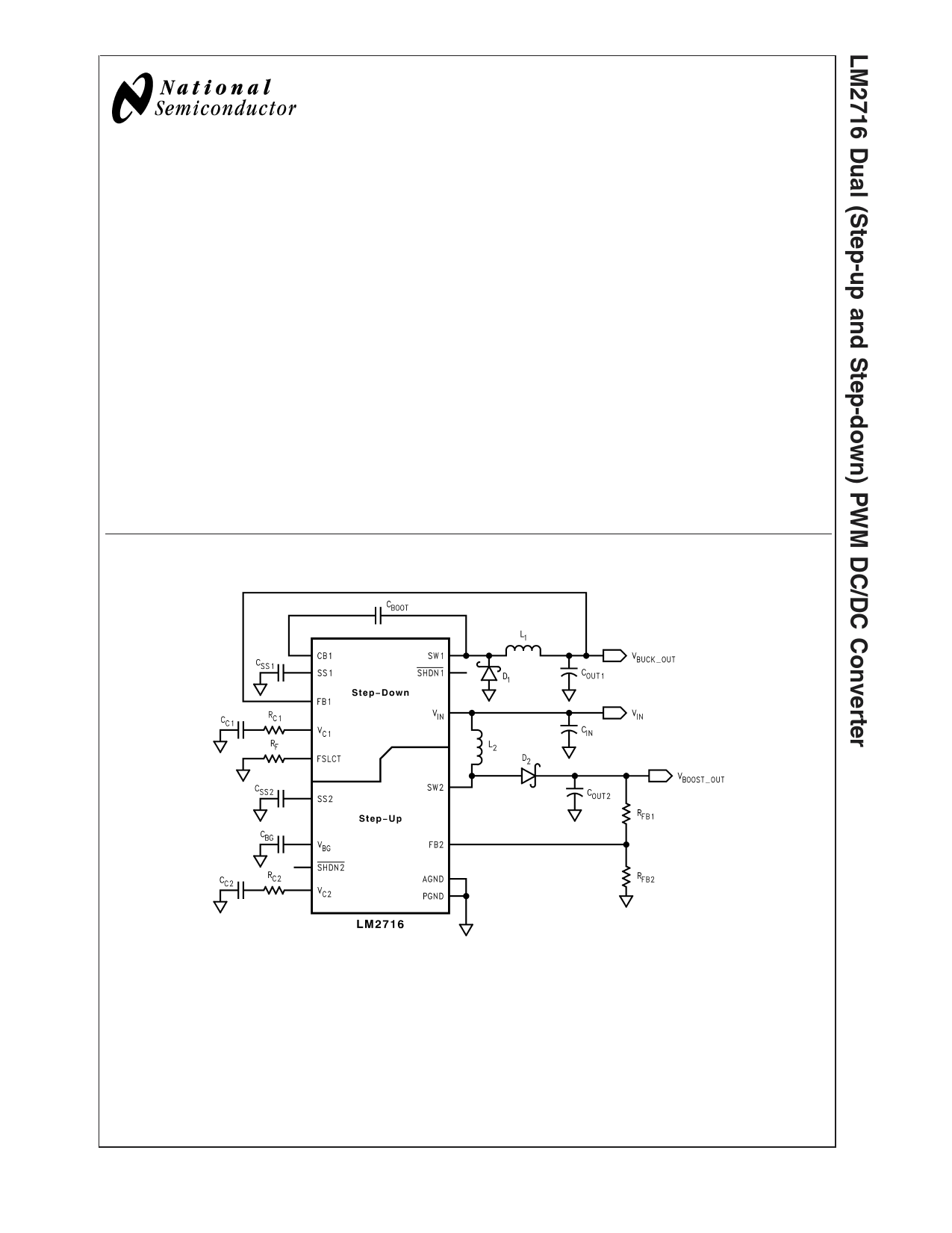
Typical Application Circuit
© 2004 National Semiconductor Corporation DS200712
20071201
www.national.com
1 page 
Absolute Maximum Ratings (Note 1)
If Military/Aerospace specified devices are required,
please contact the National Semiconductor Sales Office/
Distributors for availability and specifications.
VIN
SW1 Voltage
−0.3V to 22V
−0.3V to 22V
SW2 Voltage
−0.3V to 22V
FB1 Voltage
−0.3V to 7V
FB2 Voltage
−0.3V to 7V
VC1 Voltage
VC2 Voltage
SHDN1 Voltage
1.75V ≤ VC1 ≤ 2.25V
0.965V ≤ VC2 ≤ 1.565V
−0.3V to 7.5V
SHDN2 Voltage
−0.3V to 7.5V
SS1 Voltage
−0.3V to 2.1V
SS2 Voltage
−0.3V to 0.6V
FSLCT Voltage
AGND to 5V
CB1 Voltage
Maximum Junction Temperature
VIN + 7V (VIN = VSW)
150˚C
Power Dissipation(Note 2)
Lead Temperature
Vapor Phase (60 sec.)
Infrared (15 sec.)
ESD Susceptibility (Note 3)
Human Body Model
Machine Model
Internally Limited
300˚C
215˚C
220˚C
2kV
200V
Operating Conditions
Operating Junction
Temperature Range
(Note 4)
Storage Temperature
Supply Voltage
SW1 Voltage
SW2 Voltage
−40˚C to +125˚C
−65˚C to +150˚C
4V to 20V
20V
20V
Electrical Characteristics
Specifications in standard type face are for TJ = 25˚C and those with boldface type apply over the full Operating Tempera-
ture Range (TJ = −40˚C to +125˚C) Unless otherwise specified. VIN = 5V and IL = 0A, unless otherwise specified.
Symbol
Parameter
Conditions
Min
(Note 4)
Typ
(Note 5)
Max
(Note 4)
Units
IQ Total Quiescent Current (both Not Switching
switchers)
Switching, switch open
2.8 3.5 mA
4 4.5 mA
VBG
ICL1(Note 6)
ICL2(Note 6)
IFB1
Bandgap Voltage
Buck Switch Current Limit
Boost Switch Current Limit
Buck FB Pin Bias Current
(Note 8)
VSHDN = 0V
95% Duty Cycle (Note 7)
95% Duty Cycle (Note 7)
VFB1 = 3.3V
1.235
9
1.26
1.8
3.6
65
15
1.285
75
µA
V
A
A
µA
IFB2 Boost FB Pin Bias Current VFB2 = 1.265V
(Note 8)
27 55 nA
VIN Input Voltage Range
gm1 Buck Error Amp
∆I = 20µA
Transconductance
4 20 V
1200
µmho
gm2 Boost Error Amp
Transconductance
∆I = 5µA
175 µmho
AV1 Buck Error Amp Voltage Gain
AV2 Boost Error Amp Voltage
Gain
100 V/V
135 V/V
DMAX
FSW
ISHDN1
ISHDN2
IL1
IL2
Maximum Duty Cycle
Switching Frequency
RF = 47.5kΩ
Buck Shutdown Pin Current
Boost Shutdown Pin Current
RF = 22.6kΩ
0V < VSHDN1 < 7.5V
0V < VSHDN2 < 7.5V
Buck Switch Leakage Current VDS = 20V
Boost Switch Leakage
Current
VDS = 20V
90 95 98 %
250 300 350 kHz
500 600 700 kHz
−5 5 µA
−5 5 µA
0.2 5 µA
0.2 3 µA
RDSON1
RDSON2
Buck Switch RDSON
Boost Switch RDSON
160 mΩ
120 mΩ
5 www.national.com
5 Page 
Boost Operation
20071202
FIGURE 1. Simplified Boost Converter Diagram
(a) First Cycle of Operation (b) Second Cycle Of Operation
CONTINUOUS CONDUCTION MODE
The LM2716 contains a current-mode, PWM boost regulator.
A boost regulator steps the input voltage up to a higher
output voltage. In continuous conduction mode (when the
inductor current never reaches zero at steady state), the
boost regulator operates in two cycles.
In the first cycle of operation, shown in Figure 1 (a), the
transistor is closed and the diode is reverse biased. Energy
is collected in the inductor and the load current is supplied by
COUT.
The second cycle is shown in Figure 1 (b). During this cycle,
the transistor is open and the diode is forward biased. The
energy stored in the inductor is transferred to the load and
output capacitor.
The ratio of these two cycles determines the output voltage.
The output voltage is defined approximately as:
INTRODUCTION TO COMPENSATION
where D is the duty cycle of the switch, D and D' will be
required for design calculations.
SETTING THE OUTPUT VOLTAGE
The output voltage is set using the feedback pin and a
resistor divider connected to the output as shown in Figure 3.
The feedback pin voltage is 1.26V, so the ratio of the feed-
back resistors sets the output voltage according to the fol-
lowing equation:
20071205
FIGURE 2. (a) Inductor current. (b) Diode current.
11 www.national.com
11 Page | ||
| Páginas | Total 17 Páginas | |
| PDF Descargar | [ Datasheet LM2716MT-ADJ.PDF ] | |
Hoja de datos destacado
| Número de pieza | Descripción | Fabricantes |
| LM2716MT-ADJ | Dual (Step-up and Step-down) PWM DC/DC Converter | National Semiconductor |
| LM2716MT-ADJ | Dual (Step-up and Step-down) PWM DC/DC Converter | National Semiconductor |
| Número de pieza | Descripción | Fabricantes |
| SLA6805M | High Voltage 3 phase Motor Driver IC. |
Sanken |
| SDC1742 | 12- and 14-Bit Hybrid Synchro / Resolver-to-Digital Converters. |
Analog Devices |
|
DataSheet.es es una pagina web que funciona como un repositorio de manuales o hoja de datos de muchos de los productos más populares, |
| DataSheet.es | 2020 | Privacy Policy | Contacto | Buscar |