|
|
|
PDF LM2700 Data sheet ( Hoja de datos )
| Número de pieza | LM2700 | |
| Descripción | 600kHz/1.25MHz/ 2.5A/ Step-up PWM DC/DC Converter | |
| Fabricantes | National Semiconductor | |
| Logotipo | ||
Hay una vista previa y un enlace de descarga de LM2700 (archivo pdf) en la parte inferior de esta página. Total 17 Páginas | ||
|
No Preview Available !
October 2001
LM2700
600kHz/1.25MHz, 2.5A, Step-up PWM DC/DC Converter
General Description
The LM2700 is a step-up DC/DC converter with a 3.6A,
80mΩ internal switch and pin selectable operating fre-
quency. With the ability to produce 500mA at 8V from a
single Lithium Ion battery, the LM2700 is an ideal part for
biasing LCD displays. The LM2700 can be operated at
switching frequencies of 600kHz and 1.25MHz allowing for
easy filtering and low noise. An external compensation pin
gives the user flexibility in setting frequency compensation,
which makes possible the use of small, low ESR ceramic
capacitors at the output. The LM2700 features continuous
switching at light loads and operates with a switching quies-
cent current of 2.0mA at 600kHz and 3.0mA at 1.25MHz. The
LM2700 is available in a low profile 14-lead TSSOP package
or a 14-lead LLP package.
n Input undervoltage protection
n Adjustable output voltage up to 17.5V
n 600kHz/1.25MHz pin selectable frequency operation
n Over temperature protection
n Small 14-Lead TSSOP or LLP package
Applications
n LCD Bias Supplies
n Handheld Devices
n Portable Applications
n GSM/CDMA Phones
n Digital Cameras
Features
n 3.6A, 0.08Ω, internal switch
n Operating input voltage range of 2.2V to 12V
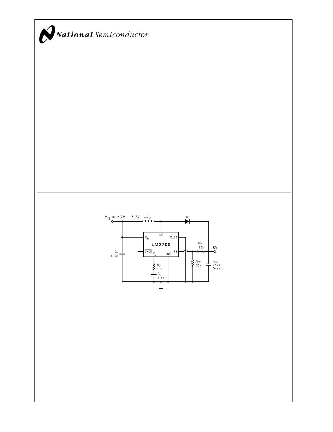
Typical Application Circuit
600 kHz Operation
20012301
© 2001 National Semiconductor Corporation DS200123
www.national.com
1 page 
Electrical Characteristics (Continued)
Note 3: The maximum allowable power dissipation is a function of the maximum junction temperature, TJ(MAX), the junction-to-ambient thermal resistance, θJA,
and the ambient temperature, TA. See the Electrical Characteristics table for the thermal resistance. The maximum allowable power dissipation at any ambient
temperature is calculated using: PD (MAX) = (TJ(MAX) − TA)/θJA. Exceeding the maximum allowable power dissipation will cause excessive die temperature, and the
regulator will go into thermal shutdown.
Note 4: The human body model is a 100 pF capacitor discharged through a 1.5kΩ resistor into each pin. The machine model is a 200pF capacitor discharged
directly into each pin.
Note 5: All limits guaranteed at room temperature (standard typeface) and at temperature extremes (bold typeface). All room temperature limits are 100% tested
or guaranteed through statistical analysis. All limits at temperature extremes are guaranteed via correlation using standard Statistical Quality Control (SQC) methods.
All limits are used to calculate Average Outgoing Quality Level (AOQL).
Note 6: Typical numbers are at 25˚C and represent the most likely norm.
Note 7: Duty cycle affects current limit due to ramp generator.
Note 8: Current limit at 0% duty cycle. See TYPICAL PERFORMANCE section for Switch Current Limit vs. VIN
Note 9: Bias current flows into FB pin.
Note 10: Does not include the bond wires. Measured directly at the die.
Note 11: Refer to National’s packaging website for more detailed thermal information and mounting techniques for the LLP and TSSOP packages.
Typical Performance Characteristics
Efficiency vs. Load Current
(VOUT = 8V, fS = 600 kHz)
Efficiency vs. Load Current
(VOUT = 8V, fS = 1.25 MHz)
20012326
Efficiency vs. Load Current
(VOUT = 5V, fS = 600 kHz)
20012325
Efficiency vs. Load Current
(VOUT = 12V, fS = 600 kHz)
20012334
5
20012335
www.national.com
5 Page 
Operation (Continued)
The phase margin can also be improved by adding CC2 as
discussed earlier in the section. The equation for ADC is
given below with additional equations required for the calcu-
lation:
mc ) 0.072fs (in V/s)
where RL is the minimum load resistance, VIN is the maxi-
mum input voltage, gm is the error amplifier transconduc-
tance found in the Electrical Characteristics table, and RD-
SON is the value chosen from the graph ’RDSON vs. VIN ’ in
the Typical Performance Characteristics section.
Application Information
Layout Considerations
The LM2700 uses two separate ground connections, PGND
for the driver and NMOS power device and AGND for the
sensitive analog control circuitry. The AGND and PGND pins
should be tied directly together at the package. The feed-
back and compensation networks should be connected di-
rectly to a dedicated analog ground plane and this ground
plane must connect to the AGND pin. If no analog ground
plane is available then the ground connections of the feed-
back and compensation networks must tie directly to the
AGND pin. Connecting these networks to the PGND can
inject noise into the system and effect performance.
The input bypass capacitor CIN, as shown in Figure 3, must
be placed close to the IC. This will reduce copper trace
resistance which effects input voltage ripple of the IC. For
additional input voltage filtering, a 100nF bypass capacitor
can be placed in parallel with CIN, close to the VIN pin, to
shunt any high frequency noise to ground. The output ca-
pacitor, COUT, should also be placed close to the IC. Any
copper trace connections for the COUT capacitor can in-
crease the series resistance, which directly effects output
voltage ripple. The feedback network, resistors RFB1 and
RFB2, should be kept close to the FB pin, and away from the
inductor, to minimize copper trace connections that can in-
ject noise into the system. Trace connections made to the
inductor and schottky diode should be minimized to reduce
power dissipation and increase overall efficiency. For more
detail on switching power supply layout considerations see
Application Note AN-1149: Layout Guidelines for Switching
Power Supplies.
FIGURE 3. 600 kHz operation, 8V output
20012331
11 www.national.com
11 Page | ||
| Páginas | Total 17 Páginas | |
| PDF Descargar | [ Datasheet LM2700.PDF ] | |
Hoja de datos destacado
| Número de pieza | Descripción | Fabricantes |
| LM2700 | 600kHz/1.25MHz/ 2.5A/ Step-up PWM DC/DC Converter | National Semiconductor |
| LM2700 | LM2700 600kHz/1.25MHz 2.5A Step-up PWM DC/DC Converter (Rev. C) | Texas Instruments |
| LM2700Q-Q1 | 600kHz/1.25MHz 2.5A Step-up PWM DC/DC Converter (Rev. A) | Texas Instruments |
| LM2702 | TFT Panel Module | National Semiconductor |
| Número de pieza | Descripción | Fabricantes |
| SLA6805M | High Voltage 3 phase Motor Driver IC. |
Sanken |
| SDC1742 | 12- and 14-Bit Hybrid Synchro / Resolver-to-Digital Converters. |
Analog Devices |
|
DataSheet.es es una pagina web que funciona como un repositorio de manuales o hoja de datos de muchos de los productos más populares, |
| DataSheet.es | 2020 | Privacy Policy | Contacto | Buscar |