|
|
|
PDF HM63021 Data sheet ( Hoja de datos )
| Número de pieza | HM63021 | |
| Descripción | 2048-word x 8-bit Line Memory | |
| Fabricantes | Renesas Technology | |
| Logotipo | ||
Hay una vista previa y un enlace de descarga de HM63021 (archivo pdf) en la parte inferior de esta página. Total 18 Páginas | ||
|
No Preview Available !
HM63021 Series
2048-word × 8-bit Line Memory
The HM63021 is a 2048-word × 8-bit static serial
access memory (SAM) with separate data inputs
and outputs. Since it has an internal address count-
er, no external address signal is required and inter-
nal addresses are scanned serially. Using five dif-
ferent address scan modes, it is applicable to FIFO
memories, double-speed conversions, 1H delay
lines, and 1H/2H delay lines for digital TV signals.
Its minimum cycle times are 28 ns and 34 ns, cor-
www.DataSrheesept4oUn.dcionmg to 8 fsc of PAL TV and NTSC TV sig-
nals. All inputs and outputs are TTL-compatible.
Features
• Five modes for various applications
• Corresponds to digital TV system with 4 fsc
sampling (PAL, NTSC)
• Decoder signal output pin (fewer external
circuits)
• Asynchronous read/write operation
— Separate address counters for read/write
— No address input required
• High speed (cycle time 28/34/45 ns (min))
• Completely static memory (no refresh required)
• 8-bit SAM with separate I/O
• Low power (250 mW typ active)
• Single 5 V supply
• TTL compatible
Ordering Information
Type No.
HM63021P-28
HM63021P-34
HM63021P-45
HM63021P28N
HM63021FP-28
HM63021FP-34
HM63021FP-45
HM63021FP28N
Cycle
time
28 ns
34 ns
45 ns
28 ns
28 ns
34 ns
45 ns
28 ns
Package
300-mil, 28-pin
plastic DIP (DP-28N)
28-pin plastic SOP
(FP-28DA)
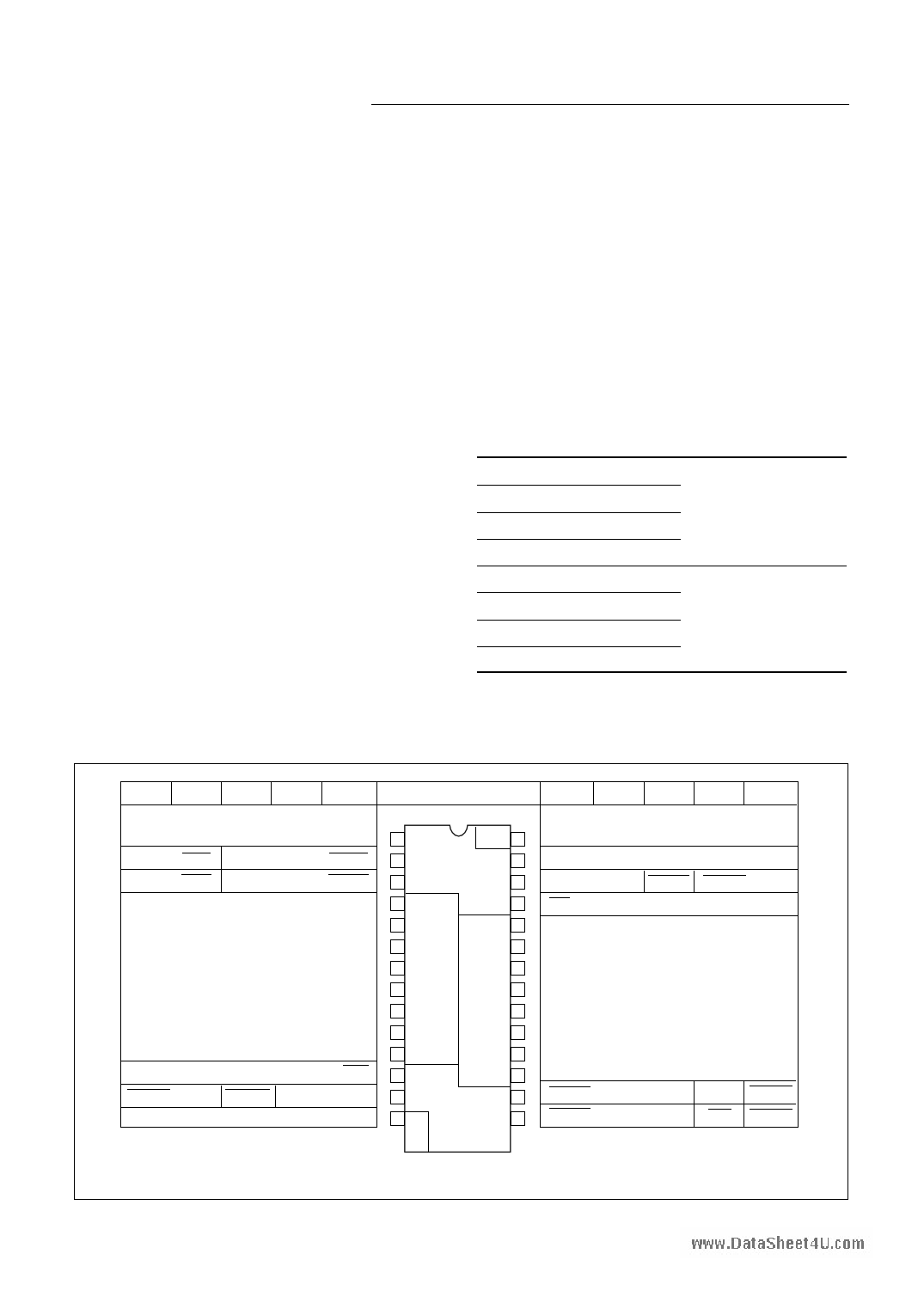
Pin Arrangement
D 1H/2H TBC DSC TBCE
CLK
RES
DEC1
WDEC
MODE1
RCLK
RRES
Din0
Din1
Din2
Din3
Din4
Din5
Din6
Din7
WE
High Z
VSS
Modes TBCE DSC TBC 1H/2H D
1 Read 28
2 control 27
3 26
4 25
5 24
6 23
7 22
8 21
9 20
10 19
11 18
12 17
13 16
14
Write 15
control
VCC
MODE2
MODE3
OE
Dout0
Dout1
Dout2
Dout3
Dout4
Dout5
Dout6
Dout7
WRES
WCLK
RDEC DEC2
DS DEC3
WT DEC4
(Top view)
1
1 page 
HM63021 Series
HM63021 Series
AC Characteristics (VCC = 5 V ± 10%*, Ta = 0 to +70°C, unless otherwise noted)
AC Test Conditions:
• Input and output timing reference levels: 1.5 V
• Input pulse levels: VSS to 3 V
• Input rise and fall times: 5 ns
Note:
5V
+10%
–5%
for
the
HM63021FP28N
and
the
HM63021P28N.
HM63021-28/34 Output Load
www.DataSheet4U.com
DEC
395 Ω
+5 V
510 Ω
30 pF*1
Dout
255 Ω
+5 V
480 Ω
30 pF*1
Dout
255 Ω
+5 V
480 Ω
5 pF*1
DEC output load
Dout output load (A)
Note: 1. Including scope and jig.
Dout output load (B)
(tOLZ, tOHZ)
HM63021-45 Output Load
DEC
495 Ω
+5 V
676 Ω
30 pF*1
Dout
294 Ω
+5 V
625 Ω
30 pF*1
Dout
294 Ω
+5 V
625 Ω
5 pF*1
DEC output load
Dout output load (A)
Note: 1. Including scope and jig.
Dout output load (B)
(tOLZ, tOHZ)
5
5 Page 
HM63021 Series
Decode Signal
HM63021 Series
When internal address counter reaches the
specified address as shown below, decode outputs
become low.
Mode
Internal
Pin No. Pin Name Address
Output Signal
Timing
Operation
TBC
13 WDEC Write 2047
After write 2047
Completion of writing on all
bits is detected.
26 RDEC
Read 2047
Output of 2046
Completion of reading from all
bits is detected.
1H/2H
13
www.DataSheet4U.com
DEC1
Read 900 (2H) Output of 900 (1H)
By inputting this signal to pin
number 3, a 901/1802-bit
delay output is obtained.
26 DEC2
Read 909 (2H) Output of 909 (1R)
By inputting this signal to pin
number 3, a 910/1820-bit
delay output is obtained.
Delay line 13
DEC1
Read 900
Output of 899
By inputting this signal to pin
number 3, a 901-bit delay
output is obtained.
Read 1810
Output of 1809
By inputting this signal to pin
number 3 after the frequency
of DEC1 is divided into two,
1811-bit delay outputs are
obtained.
26 DEC2 Read 909
Output of 908
By inputting this signal to pin
number 3, a 910-bit delay
output is obtained.
Read 1819
Output of 1818
By inputting this signal to pin
number 3 after the frequency
of DEC2 is divided into two,
1820-bit delay outputs are
obtained.
16 DEC3
Read 1134
Output of 1133
By inputting this signal to pin
number 3, 1135-bit delay
output is obtained.
I 5 DEC4
Read 1125
Output of 1124
By inputting this signal to pin
number 3, 1126-bit delay
output is obtained.
Note: When the counter is reset by a reset signal (RRES, RES, WRES), the address becomes 0.
11
11 Page | ||
| Páginas | Total 18 Páginas | |
| PDF Descargar | [ Datasheet HM63021.PDF ] | |
Hoja de datos destacado
| Número de pieza | Descripción | Fabricantes |
| HM63021 | 2048-word x 8-bit Line Memory | Renesas Technology |
| HM63021P-34 | CMOS 16K Line Memory | ETC |
| Número de pieza | Descripción | Fabricantes |
| SLA6805M | High Voltage 3 phase Motor Driver IC. |
Sanken |
| SDC1742 | 12- and 14-Bit Hybrid Synchro / Resolver-to-Digital Converters. |
Analog Devices |
|
DataSheet.es es una pagina web que funciona como un repositorio de manuales o hoja de datos de muchos de los productos más populares, |
| DataSheet.es | 2020 | Privacy Policy | Contacto | Buscar |