|
|
|
PDF LM2412 Data sheet ( Hoja de datos )
| Número de pieza | LM2412 | |
| Descripción | Monolithic Triple 2.8 ns CRT Driver | |
| Fabricantes | National Semiconductor | |
| Logotipo | ||
Hay una vista previa y un enlace de descarga de LM2412 (archivo pdf) en la parte inferior de esta página. Total 11 Páginas | ||
|
No Preview Available !
December 1999
LM2412
Monolithic Triple 2.8 ns CRT Driver
General Description
The LM2412 is an integrated high voltage CRT driver circuit
designed for use in high resolution color monitor applica-
tions. The IC contains three high input impedance, wide
band amplifiers which directly drive the RGB cathodes of a
CRT. Each channel has its gain internally set to −14 and can
drive CRT capacitive loads as well as resistive loads pre-
sented by other applications, limited only by the package’s
power dissipation. The LM2412 is a low power alternative of
the LM2402
The IC is packaged in an industry standard 11 lead TO-220
molded plastic power package. See thermal considerations
section for heat sinking requirements.
Features
n Rise/fall times typically 2.8 ns with 8 pF load at 40 VPP
n Lower power than LM2402 with the same bandwidth
n Well matched with LM2202 video preamps
n Output swing capability: 50 VPP for VCC = 80V
n 1V to 5V input range
n Stable with 0-20 pF capacitive loads and inductive
peaking networks
n Convenient TO-220 staggered lead package style
n Standard LM240X family pinout which is designed for
easy PCB layout
Applications
n CRT driver for color monitors with display resolutions up
to 1600 x 1200 with 85 Hz refresh rate
n Pixel clock frequency up to 200 MHz
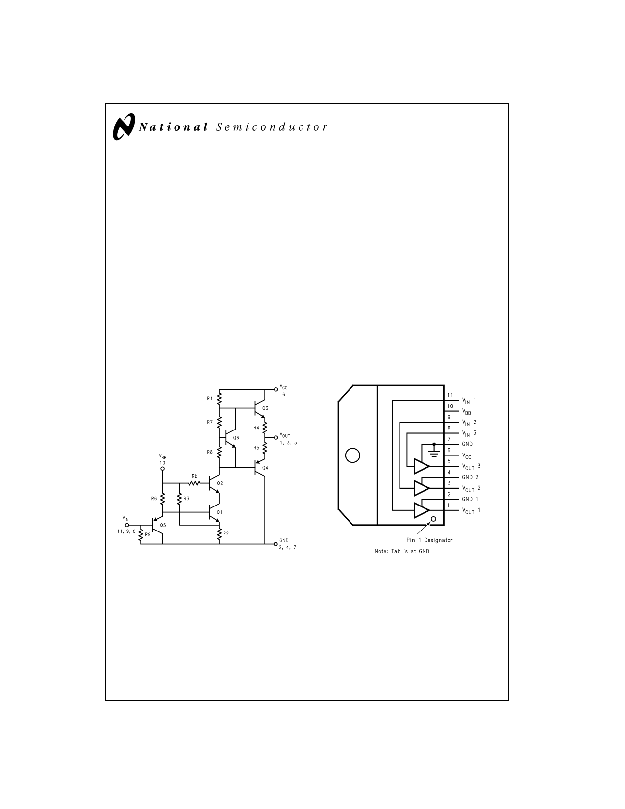
Schematic and Connection Diagrams
DS101298-1
FIGURE 1. Simplified Schematic Diagram
(One Channel)
DS101298-2
Top View
Order Number LM2412T
See NS package Number
© 1999 National Semiconductor Corporation DS101298
www.national.com
1 page 
Application Hints (Continued)
above 300 MHz. Air core inductors from J.W. Miller Magnet-
ics (part #75F518MPC) were used for optimizing the perfor-
mance of the device in the NSC application board. The val-
ues shown in Figure 9 can be used as a good starting point
for the evaluation of the LM2412.
Effect of Load Capacitance
The output rise and fall times as well as overshoot will vary
as the load capacitance varies. The values of the output cir-
cuit (R1, R2 and L1 in Figure 9) should be chosen based on
the nominal load capacitance. Once this is done the perfor-
mance of the design can be checked by varying the load
based on what the expected variation will be during produc-
tion.
4. Divide the result from step 3 by 0.72. For 100 MHz, the
result is 18.1W.
5. Multiply the result in 4 by the new active time percent-
age.
6. Multiply 2.7W by the new inactive time.
7. Add together the results of steps 5 and 6. This is the ex-
pected power dissipation for the LM2412 in the design-
er’s application.
The LM2412 case temperature must be maintained below
100˚C. If the maximum expected ambient temperature is
70˚C and the maximum power dissipation is 13.8W (from
Figure 6. 100MHz) then a maximum heat sink thermal resis-
tance can be calculated:
Effect of Offset
Figure 7 shows the variation in rise and fall times when the
output offset of the device is varied from 35 to 55 VDC. The
rise and fall times show about the same overall variation.
The slightly slower fall time is fastest near the center point of
45V, making this the optimum operating point. At the low and
high output offset range, the characteristic of rise/fall time is
slower due to the saturation of Q3 and Q4. The recovery
time of the output transistors takes longer coming out of
saturation thus slows down the rise and fall times.
THERMAL CONSIDERATIONS
Figure 4 shows the performance of the LM2412 in the test
circuit shown in Figure 2 as a function of case temperature.
Figure 4 shows that both the rise and fall times of the
LM2412 become slightly longer as the case temperature in-
creases from 40˚C to 125˚C. In addition to exceeding the
safe operating temperature, the rise and fall times will typi-
cally exceed 3 nsec. Please note that the LM2412 is never
to be operated over a case temperature of 100˚C. In addi-
tion to exceeding the safe operating temperature, the rise
and fall times will typically exceed 3 nsec.
Figure 6 shows the total power dissipation of the LM2412 vs.
Frequency when all three channels of the device are driving
an 8 pF load. Typically the active time is about 72% of the to-
tal time for one frame. Worst case power dissipation is when
a one on, one off pixel is displayed over the active time of the
video input. This is the condition used to measure the total
power disspation of the LM2412 at different input frequen-
cies. Figure 6 gives all the information a monitor designer
normally needs for worst case power dissipation. However, if
the designer wants to calculate the power dissipation for an
active time different from 72%, this can be done using the in-
formation in Figure 14. The recommended input black level
voltage is 1.9V. From Figure 14, if a 1.9V input is used for
the black level, then power dissipation during the inactive
video time is 2.7W. This includes both the 80V and 12V sup-
plies.
If the monitor designer chooses to calculate the power dissi-
pation for the LM2412 using an active video time different
from 72%, then he needs to use the following steps when us-
ing a 1.9V input black level:
1. Multiply the black level power dissipation, 2.7W, by 0.28,
the result is 0.8W.
2. Choose the maximum frequency to be used. A typical
application would use 100 MHz, or a 200 MHz pixel
clock. The power dissipation is 13.8W.
3. Subtract the 0.8W from the power dissipation from Fig-
ure 6. For 100 MHz this would be 13.8 – 0.8 = 13.0W.
TYPICAL APPLICATION
A typical application of the LM2412 is shown in Figure 10.
Used in conjunction with three LM2202s, a complete video
channel from monitor input to CRT cathode can be achieved.
Performance is excellent for resolutions up to 1600 x 1200
and pixel clock frequencies at 200 MHz. Figure 10 is the
schematic for the NSC demonstration board that can be
used to evaluate the LM2202/LM2412 combination in a
monitor.
PC Board Layout Considerations
For optimum performance, an adequate ground plane, isola-
tion between channels, good supply bypassing and minimiz-
ing unwanted feedback are necessary. Also, the length of the
signal traces from the preamplifier to the LM2412 and from
the LM2412 to the CRT cathode should be as short as pos-
sible. The red video trace from the buffer transistor to the
LM2412 input is about the absolute maximum length one
should consider on a PCB layout. If possible the traces
should actually be shorter than the red video trace. The fol-
lowing references are recommended for video board design-
ers:
Ott, Henry W., “Noise Reduction Techniques in Electronic
Systems”, John Wiley & Sons, New York, 1976.
“Guide to CRT Video Design”, National Semiconductor Appli-
cation Note 861.
“Video Amplifier Design for Computer Monitors”, National
Semiconductor Application Note 1013.
Pease, Robert A., “Troubleshooting Analog Circuits”,
Butterworth-Heinemann, 1991.
Because of its high small signal bandwidth, the part may os-
cillate in a monitor if feedback occurs around the video chan-
nel through the chassis wiring. To prevent this, leads to the
video amplifier input circuit should be shielded, and input cir-
cuit wiring should be spaced as far as possible from output
circuit wiring.
NSC Demonstration Board
Figures 11, 12 show routing and component placement on
the NSC LM2202/2412 demonstration board. The schematic
of the board is shown in Figure 10. This board provides a
good example of a layout that can be used as a guide for fu-
ture layouts. Note the location of the following components:
• C47 - VCC bypass capacitor, located very close to pin 6
and ground pins. (Figure 12)
• C49 - VBB bypass capacitor, located close to pin 10 and
ground. (Figure 12)
5 www.national.com
5 Page 
Physical Dimensions inches (millimeters) unless otherwise noted
11 Lead Molded TO-220
NS Package Number TA11B
Order Number LM2412T
LIFE SUPPORT POLICY
NATIONAL’S PRODUCTS ARE NOT AUTHORIZED FOR USE AS CRITICAL COMPONENTS IN LIFE SUPPORT
DEVICES OR SYSTEMS WITHOUT THE EXPRESS WRITTEN APPROVAL OF THE PRESIDENT AND GENERAL
COUNSEL OF NATIONAL SEMICONDUCTOR CORPORATION. As used herein:
1. Life support devices or systems are devices or
systems which, (a) are intended for surgical implant
into the body, or (b) support or sustain life, and
whose failure to perform when properly used in
accordance with instructions for use provided in the
labeling, can be reasonably expected to result in a
significant injury to the user.
2. A critical component is any component of a life
support device or system whose failure to perform
can be reasonably expected to cause the failure of
the life support device or system, or to affect its
safety or effectiveness.
National Semiconductor
Corporation
Americas
Tel: 1-800-272-9959
Fax: 1-800-737-7018
Email: [email protected]
www.national.com
National Semiconductor
Europe
Fax: +49 (0) 1 80-530 85 86
Email: [email protected]
Deutsch Tel: +49 (0) 1 80-530 85 85
English Tel: +49 (0) 1 80-532 78 32
Français Tel: +49 (0) 1 80-532 93 58
Italiano Tel: +49 (0) 1 80-534 16 80
National Semiconductor
Asia Pacific Customer
Response Group
Tel: 65-2544466
Fax: 65-2504466
Email: [email protected]
National Semiconductor
Japan Ltd.
Tel: 81-3-5639-7560
Fax: 81-3-5639-7507
National does not assume any responsibility for use of any circuitry described, no circuit patent licenses are implied and National reserves the right at any time without notice to change said circuitry and specifications.
11 Page | ||
| Páginas | Total 11 Páginas | |
| PDF Descargar | [ Datasheet LM2412.PDF ] | |
Hoja de datos destacado
| Número de pieza | Descripción | Fabricantes |
| LM2412 | Monolithic Triple 2.8 ns CRT Driver | National Semiconductor |
| LM2412 | LM2412 Monolithic Triple 2.8 ns CRT Driver (Rev. A) | Texas Instruments |
| LM2412A | LM2412A Monolithic Triple 2.8 ns CRT Driver (Rev. A) | Texas Instruments |
| LM2412T | Monolithic Triple 2.8 ns CRT Driver | National Semiconductor |
| Número de pieza | Descripción | Fabricantes |
| SLA6805M | High Voltage 3 phase Motor Driver IC. |
Sanken |
| SDC1742 | 12- and 14-Bit Hybrid Synchro / Resolver-to-Digital Converters. |
Analog Devices |
|
DataSheet.es es una pagina web que funciona como un repositorio de manuales o hoja de datos de muchos de los productos más populares, |
| DataSheet.es | 2020 | Privacy Policy | Contacto | Buscar |