|
|
|
PDF 41C16256 Data sheet ( Hoja de datos )
| Número de pieza | 41C16256 | |
| Descripción | IS41C16256 | |
| Fabricantes | Integrated Circuit Solution | |
| Logotipo | ||
Hay una vista previa y un enlace de descarga de 41C16256 (archivo pdf) en la parte inferior de esta página. Total 20 Páginas | ||
|
No Preview Available !
www.DaIStaS4he1eCt4U1.c6om256
IS41LV16256
256K x 16 (4-MBIT) DYNAMIC RAM
WITH EDO PAGE MODE
FEATURES
• Extended Data-Out (EDO) Page Mode access cycle
• TTL compatible inputs and outputs; tristate I/O
• Refresh Interval: 512 cycles /8 ms
• Refresh Mode: RAS-Only, CAS-before-RAS (CBR),
Hidden
• Single power supply:
5V ± 10% (IS41C16256)
3.3V ± 10% (IS41LV16256)
• Byte Write and Byte Read operation via two CAS
• Industrial Temperature Range -40oC to 85oC
DESCRIPTION
The ICSI IS41C16256 and IS41LV16256 is a 262,144 x 16-
bit high-performance CMOS Dynamic Random Access Memo-
ries. The IS41C16256 offer an accelerated cycle access
called EDO Page Mode. EDO Page Mode allows 512 random
accesses within a single row with access cycle time as short
as 10 ns per 16-bit word. The Byte Write control, of upper and
lower byte, makes the IS41C16256 ideal for use in
16-, 32-bit wide data bus systems.
These features make the IS41C16256and IS41LV16256 ideally
suited for high-bandwidth graphics, digital signal processing,
high-performance computing systems, and peripheral
applications.
KEY TIMING PARAMETERS
Parameter
Max. RAS Access Time (tRAC)
Max. CAS Access Time (tCAC)
Max. Column Address Access Time (tAA)
Min. EDO Page Mode Cycle Time (tPC)
Min. Read/Write Cycle Time (tRC)
The IS41C16256 is packaged in a 40-pin 400mil SOJ and
400mil TSOP-2.
-25(5V)
-35
-50
-60 Unit
25 35 50 60 ns
10 10 14 15 ns
12 18 25 30 ns
10 12 20 25 ns
45 60 90 110 ns
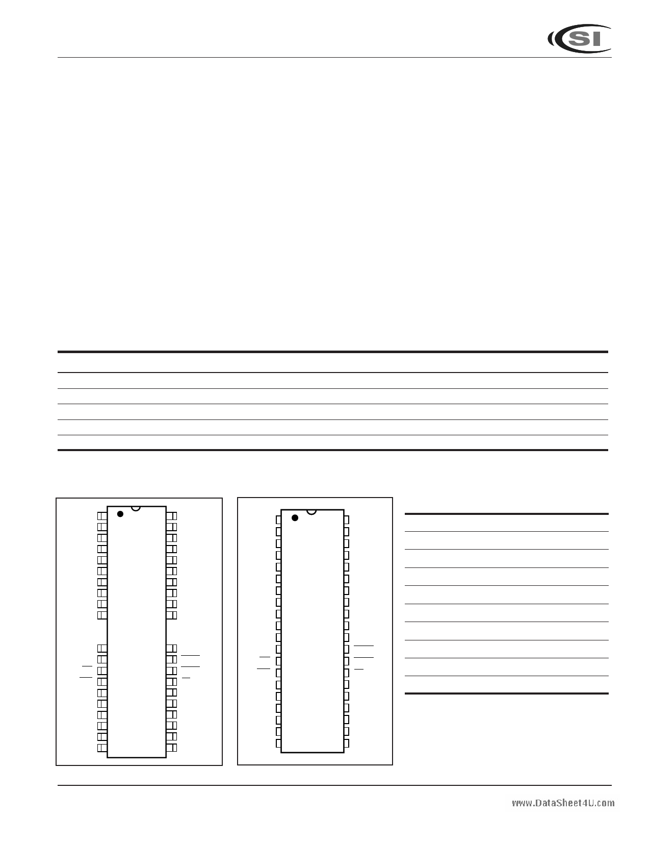
PIN CONFIGURATIONS
40-Pin TSOP-2
VCC
I/O0
I/O1
I/O2
I/O3
VCC
I/O4
I/O5
I/O6
I/O7
1
2
3
4
5
6
7
8
9
10
40 GND
39 I/O15
38 I/O14
37 I/O13
36 I/O12
35 GND
34 I/O11
33 I/O10
32 I/O9
31 I/O8
NC
NC
WE
RAS
NC
A0
A1
A2
A3
VCC
11
12
13
14
15
16
17
18
19
20
30 NC
29 LCAS
28 UCAS
27 OE
26 A8
25 A7
24 A6
23 A5
22 A4
21 GND
40-Pin SOJ
VCC
I/O0
I/O1
I/O2
I/O3
VCC
I/O4
I/O5
I/O6
I/O7
NC
NC
WE
RAS
NC
A0
A1
A2
A3
VCC
1
2
3
4
5
6
7
8
9
10
11
12
13
14
15
16
17
18
19
20
40 GND
39 I/O15
38 I/O14
37 I/O13
36 I/O12
35 GND
34 I/O11
33 I/O10
32 I/O9
31 I/O8
30 NC
29 LCAS
28 UCAS
27 OE
26 A8
25 A7
24 A6
23 A5
22 A4
21 GND
PIN DESCRIPTIONS
A0-A8
I/O0-15
WE
OE
RAS
UCAS
LCAS
Vcc
GND
NC
Address Inputs
Data Inputs/Outputs
Write Enable
Output Enable
Row Address Strobe
Upper Column Address Strobe
Lower Column Address Strobe
Power
Ground
No Connection
ICSI reserves the right to make changes to its products at any time without notice in order to improve design and supply the best possible product. We assume no responsibility for any errors
which may appear in this publication. © Copyright 2000, Integrated Circuit Solution Inc.
Integrated Circuit Solution Inc.
DR001-0E 01/25/2002
1
1 page 
www.DaIStaS4he1eCt4U1.c6om256
IS41LV16256
ABSOLUTE MAXIMUM RATINGS(1)
Symbol Parameters
Rating Unit
VT
Voltage on Any Pin Relative to GND
5V –1.0 to +7.0 V
3.3V –0.5 to +4.6
VCC Supply Voltage
5V
3.3V
–1.0 to +7.0 V
–0.5 to +4.6
IOUT Output Current
50 mA
PD Power Dissipation
1W
TA Commercial Operation Temperature
Industrial Operationg Temperature
0 to +70 °C
–40 to +85 °C
TSTG
Storage Temperature
–55 to +125 °C
Note:
1. Stress greater than those listed under ABSOLUTE MAXIMUM RATINGS may cause permanent
damage to the device. This is a stress rating only and functional operation of the device at these
or any other conditions above those indicated in the operational sections of this specification is
not implied. Exposure to absolute maximum rating conditions for extended periods may affect
reliability.
RECOMMENDED OPERATING CONDITIONS (Voltages are referenced to GND.)
Symbol
VCC
VIH
VIL
TA
Parameter
Supply Voltage
Input High Voltage
Input Low Voltage
Commercial Ambient Temperature
Industrial Ambient Temperature
5V
3.3V
5V
3.3V
5V
3.3V
Min.
4.5
3.0
2.4
2.0
–1.0
–0.3
0
–40
Typ.
5.0
3.3
—
—
—
—
—
—
Max.
5.5
3.6
VCC + 1.0
VCC + 0.3
0.8
0.8
70
85
Unit
V
V
V
°C
°C
CAPACITANCE(1,2)
Symbol
CIN1
CIN2
CIO
Parameter
Input Capacitance: A0-A8
Input Capacitance: RAS, UCAS, LCAS, WE, OE
Data Input/Output Capacitance: I/O0-I/O15
Max.
5
7
7
Unit
pF
pF
pF
Notes:
1. Tested initially and after any design or process changes that may affect these parameters.
2. Test conditions: TA = 25°C, f = 1 MHz.
Integrated Circuit Solution Inc.
DR001-0E 01/25/2002
5
5 Page 
www.DaIStaS4he1eCt4U1.c6om256
IS41LV16256
EARLY WRITE CYCLE (OE = DON'T CARE)
RAS
tCRP
UCAS/LCAS
tASR
ADDRESS
Row
WE
I/O
tRAS
tRC
tRCD
tCSH
tRSH
tCAS tCLCH
tRAD
tRAH
tASC
tAR
tRAL
tCAH
tACH
Column
tWCR
tWCS
tCWL
tRWL
tWCH
tWP
tDHR
tDS
tDH
Valid Data
tRP
Row
Don’t Care
Integrated Circuit Solution Inc.
DR001-0E 01/25/2002
11
11 Page | ||
| Páginas | Total 20 Páginas | |
| PDF Descargar | [ Datasheet 41C16256.PDF ] | |
Hoja de datos destacado
| Número de pieza | Descripción | Fabricantes |
| 41C16256 | IS41C16256 | Integrated Circuit Solution |
| 41C16257 | 256K x 16 (4-MBIT) DYNAMIC RAM WITH FAST PAGE MODE | Integrated Silicon Solution Inc |
| Número de pieza | Descripción | Fabricantes |
| SLA6805M | High Voltage 3 phase Motor Driver IC. |
Sanken |
| SDC1742 | 12- and 14-Bit Hybrid Synchro / Resolver-to-Digital Converters. |
Analog Devices |
|
DataSheet.es es una pagina web que funciona como un repositorio de manuales o hoja de datos de muchos de los productos más populares, |
| DataSheet.es | 2020 | Privacy Policy | Contacto | Buscar |