|
|
PDF LV5608LP Data sheet ( Hoja de datos )
| Número de pieza | LV5608LP | |
| Descripción | Bi-CMOS LSI | |
| Fabricantes | Sanyo Semicon Device | |
| Logotipo | ||
Hay una vista previa y un enlace de descarga de LV5608LP (archivo pdf) en la parte inferior de esta página. Total 8 Páginas | ||
|
No Preview Available !
www.DataSheet4U.com
Ordering number : ENA0691
LV5608LP
Bi-CMOS LSI
For CCD
Charge pump power supply
Overview
The LV5608LP is charge pump power supply for CCD.
Functions
• The charge pump boosts the +3.3V input by multiplying with +6, then by -3 to regulate the voltage to the specified level.
• The output voltage is +15V, -7.5V necessary for CCD.
• Soft start function incorporated, which reduces the inrush current at start of charge pump.
• Short-circuit protection function incorporated.
• Four types of operating frequency selectable.
Specifications
Absolute Maximum Ratings at Ta = 25°C
Parameter
Symbol
Conditions
Maximum supply voltage
Allowable power dissipation
VDD max
Pd max
with specified substrate *1
Operating temperature
Topr
Storage temperature
Tstg
*1 : Specified substrate : 40×50×0.8mm3, glass epoxy four-layer (2S2P) board
Ratings
3.5
0.8
-20 to +80
-40 to +125
Allowable Operating Ratings at Ta = 25°C, PGND = 0V
Parameter
Symbol
Conditions
min
Supply voltage
Input CLK frequency
VDD
CKIN
SEL=H *2
3.0
0.1
Input High voltage
Input Low voltage
VINH
VINL
EN pin
EN pin
0.7VDD
-0.1
*2 : Note that the charge pump frequency should be adjusted with S0/S1 so that it becomes 2 MHz or less.
Ratings
typ
3.3
max
3.45
8
VDD
0.4
Unit
V
W
°C
°C
Unit
V
MHz
V
V
Any and all SANYO Semiconductor products described or contained herein do not have specifications
that can handle applications that require extremely high levels of reliability, such as life-support systems,
aircraft's control systems, or other applications whose failure can be reasonably expected to result in
serious physical and/or material damage. Consult with your SANYO Semiconductor representative
nearest you before using any SANYO Semiconductor products described or contained herein in such
applications.
SANYO Semiconductor assumes no responsibility for equipment failures that result from using products
at values that exceed, even momentarily, rated values (such as maximum ratings, operating condition
ranges, or other parameters) listed in products specifications of any and all SANYO Semiconductor
products described or contained herein.
32207 MS PC 20060728-S00004 No.A0691-1/8
1 page 
www.DataSheet4U.com
LV5608LP
Short-circuit Protection
VH and VL output pins incorporate the short-circuit protection function.
When the output pins are short-circuited to allow the large current to flow, IC is latched OFF to interrupt output.
To reset from the interrupted state, set the EN pin to L, then reset it again to H.
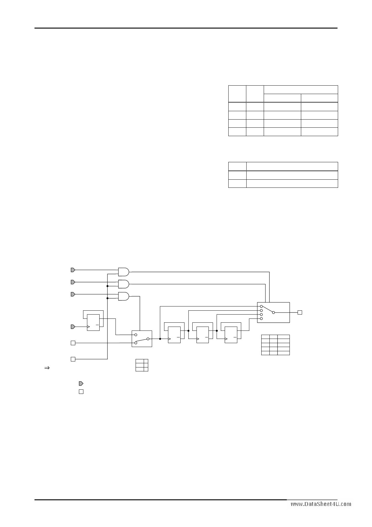
Frequency Selection
The charge pump operating frequency can be changed with S0 and S1
logics.
For light load, the reactive load can be reduced by lowering the
operating frequency.
SEL logic also enables synchronous operation with external CLK.
The charge pump is operated with the frequency equivalent to 1/2 of
input CLK.
(The IC internal oscillator is used for the sequence, so that it is
normally ON regardless of SEL.
S0 S1
LL
HL
LH
HH
CP operating frequency
SEL=L
SEL=H
1MHz
1/2 CLK
500kHz
1/4 CLK
250kHz
1/8 CLK
125kHz
1/16 CLK
For minimum 9.4ms after startup with the EN signal set to H, the IC
internal clock is used to operate the charge pump with 1 MHz regardless
of the input of SEL, S0, and S1 pins. After the 9.4ms(min) period, the
charge pump frequency is changed over according to the state of SEL,
S0, and S1 pins. The changeover frequency is set as shown in the table
right.
SEL
L IC internal oscillator
H Synchronous operation with external CLK
Internal Equivalent Circuit
S0 pin
S1 pin
SEL pin
CLK pin
DQ
Q
Internal
1MHz
VH regulator start
signal
L H in 9.4 ms (min) after EN = H
B
Y
A
2-input multiplexer
Truth Table
SEL Y
LA
HB
DQ
Q
External signal input pin
Internal signal
DQ
Q
DQ
Q
clk
clk/2
clk/4
clk/8
Y
4-input multiplexer
Truth Table
S0 S1 Y
L L clk
H L clk/2
L H clk/4
H H clk/8
Charge pump
clock
No.A0691-5/8
5 Page | ||
| Páginas | Total 8 Páginas | |
| PDF Descargar | [ Datasheet LV5608LP.PDF ] | |
Hoja de datos destacado
| Número de pieza | Descripción | Fabricantes |
| LV5608LP | Bi-CMOS LSI | Sanyo Semicon Device |
| Número de pieza | Descripción | Fabricantes |
| SLA6805M | High Voltage 3 phase Motor Driver IC. |
Sanken |
| SDC1742 | 12- and 14-Bit Hybrid Synchro / Resolver-to-Digital Converters. |
Analog Devices |
|
DataSheet.es es una pagina web que funciona como un repositorio de manuales o hoja de datos de muchos de los productos más populares, |
| DataSheet.es | 2020 | Privacy Policy | Contacto | Buscar |
