|
|
|
PDF FDS8958 Data sheet ( Hoja de datos )
| Número de pieza | FDS8958 | |
| Descripción | Dual N & P-Channel PowerTrench MOSFET | |
| Fabricantes | Fairchild Semiconductor | |
| Logotipo | ||
Hay una vista previa y un enlace de descarga de FDS8958 (archivo pdf) en la parte inferior de esta página. Total 8 Páginas | ||
|
No Preview Available !
www.DataSheet4U.com
October 2004
FDS8958
Dual N & P-Channel PowerTrench® MOSFET
General Description
These dual N- and P-Channel enhancement mode
power field effect transistors are produced using
Fairchild Semiconductor’s advanced PowerTrench
process that has been especially tailored to minimize
on-state ressitance and yet maintain superior switching
performance.
These devices are well suited for low voltage and
battery powered applications where low in-line power
loss and fast switching are required.
Features
• Q1: N-Channel
7.0A, 30V RDS(on) = 0.028Ω @ VGS = 10V
RDS(on) = 0.040Ω @ VGS = 4.5V
• Q2: P-Channel
-5A, -30V RDS(on) = 0.052Ω @ VGS = -10V
RDS(on) = 0.080Ω @ VGS = -4.5V
• Fast switching speed
• High power and handling capability in a widely
used surface mount package
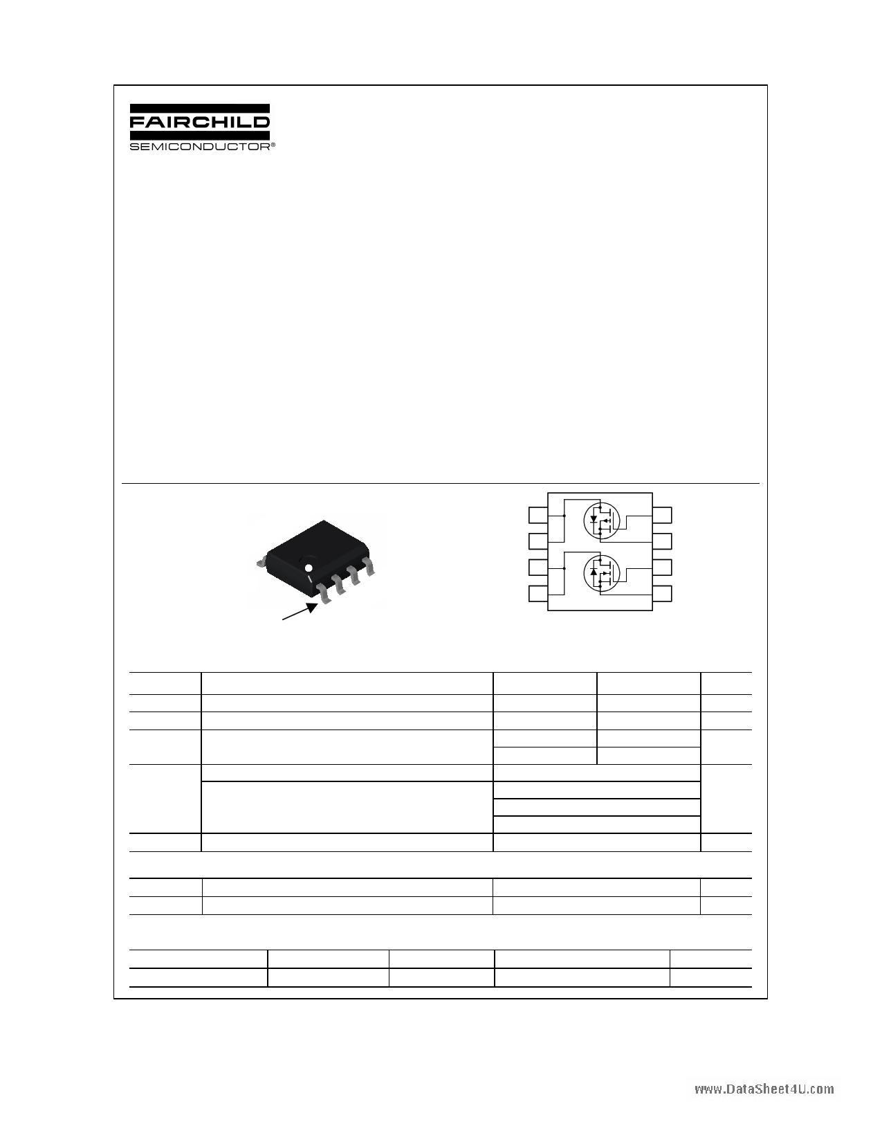
DD2
DD2
DD1
DD1
SO-8
Pin 1 SO-8
G2
S2 G
G1 S
S1 S
S
Q2
5
6
Q1
7
8
4
3
2
1
Absolute Maximum Ratings TA = 25°C unless otherwise noted
Symbol
Parameter
VDSS
VGSS
Drain-Source Voltage
Gate-Source Voltage
ID Drain Current - Continuous
- Pulsed
(Note 1a)
PD Power Dissipation for Dual Operation
Power Dissipation for Single Operation
(Note 1a)
(Note 1b)
(Note 1c)
TJ, TSTG
Operating and Storage Junction Temperature Range
Thermal Characteristics
RθJA Thermal Resistance, Junction-to-Ambient
RθJC Thermal Resistance, Junction-to-Case
(Note 1a)
(Note 1)
Package Marking and Ordering Information
Device Marking
Device
Reel Size
FDS8958
FDS8958
13”
Q1 Q2
30 30
±20 ±20
7 -5
20 -20
2
1.6
1
0.9
-55 to +150
78
40
Units
V
V
A
W
°C
°C/W
°C/W
Tape width
12mm
Quantity
2500 units
©2004 Fairchild Semiconductor Corporation
FDS8958 Rev A(W)
1 page 
www.DataSheet4U.com
Typical Characteristics: Q1
10
ID =7A
8
6
VDS = 5V
15V
10V
4
2
0
0 4 8 12 16
Qg, GATE CHARGE (nC)
Figure 7. Gate Charge Characteristics.
100
RDS(ON) LIMIT
10
1
VGS = 10V
SINGLE PULSE
0.1 RθJA = 135oC/W
TA = 25oC
100µs
1ms
10ms
100ms
1s
10s
DC
0.01
0.1
1 10
VDS, DRAIN-SOURCE VOLTAGE (V)
100
Figure 9. Maximum Safe Operating Area.
1200
900
600
CISS
f = 1MHz
VGS = 0 V
300
0
0.0
COSS
CRSS
5.0 10.0 15.0
VDS, DRAIN TO SOURCE VOLTAGE (V)
20.0
Figure 8. Capacitance Characteristics.
50
SINGLE PULSE
40 RθJA = 135°C/W
TA = 25°C
30
20
10
0
0.001
0.01
0.1 1 10
t1, TIME (sec)
100 1000
Figure 10. Single Pulse Maximum
Power Dissipation.
FDS8958 Rev A(W)
5 Page | ||
| Páginas | Total 8 Páginas | |
| PDF Descargar | [ Datasheet FDS8958.PDF ] | |
Hoja de datos destacado
| Número de pieza | Descripción | Fabricantes |
| FDS8958 | Dual N & P-Channel PowerTrench MOSFET | Fairchild Semiconductor |
| FDS8958A | Dual N & P-Channel Enhancement Mode Field Effect Transistor | Fairchild Semiconductor |
| FDS8958A_F085 | Dual N & P-Channel PowerTrench MOSFET | Fairchild Semiconductor |
| FDS8958B | MOSFET ( Transistor ) | Fairchild Semiconductor |
| Número de pieza | Descripción | Fabricantes |
| SLA6805M | High Voltage 3 phase Motor Driver IC. |
Sanken |
| SDC1742 | 12- and 14-Bit Hybrid Synchro / Resolver-to-Digital Converters. |
Analog Devices |
|
DataSheet.es es una pagina web que funciona como un repositorio de manuales o hoja de datos de muchos de los productos más populares, |
| DataSheet.es | 2020 | Privacy Policy | Contacto | Buscar |