|
|
|
PDF ADS1218 Data sheet ( Hoja de datos )
| Número de pieza | ADS1218 | |
| Descripción | 24-Bit ANALOG-TO-DIGITAL CONVERTER | |
| Fabricantes | Burr-Brown | |
| Logotipo | ||
Hay una vista previa y un enlace de descarga de ADS1218 (archivo pdf) en la parte inferior de esta página. Total 30 Páginas | ||
|
No Preview Available !
www.DataSheet4U.com
ADS1218
ADS1218
SBAS187 – SEPTEMBER 2001
8-Channel, 24-Bit
ANALOG-TO-DIGITAL CONVERTER
with FLASH Memory
FEATURES
q 24 BITS NO MISSING CODES
q 0.0015% INL
q 22 BITS EFFECTIVE RESOLUTION
(PGA = 1), 19 BITS (PGA = 128)
q 4K BYTES OF FLASH MEMORY
PROGRAMMABLE FROM 2.7V TO 5.25V
q PGA FROM 1 TO 128
q SINGLE CYCLE SETTLING MODE
q PROGRAMMABLE DATA OUTPUT RATES
UP TO 1kHz
q PRECISION ON-CHIP 1.25V/2.5V REFERENCE:
ACCURACY: 0.2%
DRIFT: 5ppm/°C
q EXTERNAL DIFFERENTIAL REFERENCE
OF 0.1V TO 2.5V
q ON-CHIP CALIBRATION
q PIN COMPATIBLE WITH ADS1216
q SPI™ COMPATIBLE
q 2.7V TO 5.25V
q < 1mW POWER CONSUMPTION
DESCRIPTION
The ADS1218 is a precision, wide dynamic range, delta-sigma, Analog-to-
Digital (A/D) converter with 24-bit resolution and FLASH memory operating
from 2.7V to 5.25V supplies. The delta-sigma, A/D converter provides up to
24 bits of no missing code performance and effective resolution of 22 bits.
The eight input channels are multiplexed. Internal buffering can be selected
to provide a very high input impedance for direct connection to transducers
or low-level voltage signals. Burn out current sources are provided that allow
for the detection of an open or shorted sensor. An 8-bit Digital-to-Analog (D/
A) converter provides an offset correction with a range of 50% of the FSR
(Full-Scale Range).
The PGA (Programmable Gain Amplifier) provides selectable gains of 1 to
128 with an effective resolution of 19 bits at a gain of 128. The A/D
conversion is accomplished with a second-order delta-sigma modulator and
programmable sinc filter. The reference input is differential and can be used
for ratiometric conversion. The on-board current DACs (Digital-to-Analog
Converters) operate independently with the maximum current set by an
external resistor.
The serial interface is SPI compatible. Eight bits of digital I/O are also provided
thatcanbeusedforinputoroutput.TheADS1218isdesignedforhigh-resolution
measurement applications in smart transmitters, industrial process control, weight
scales, chromatography, and portable instrumentation.
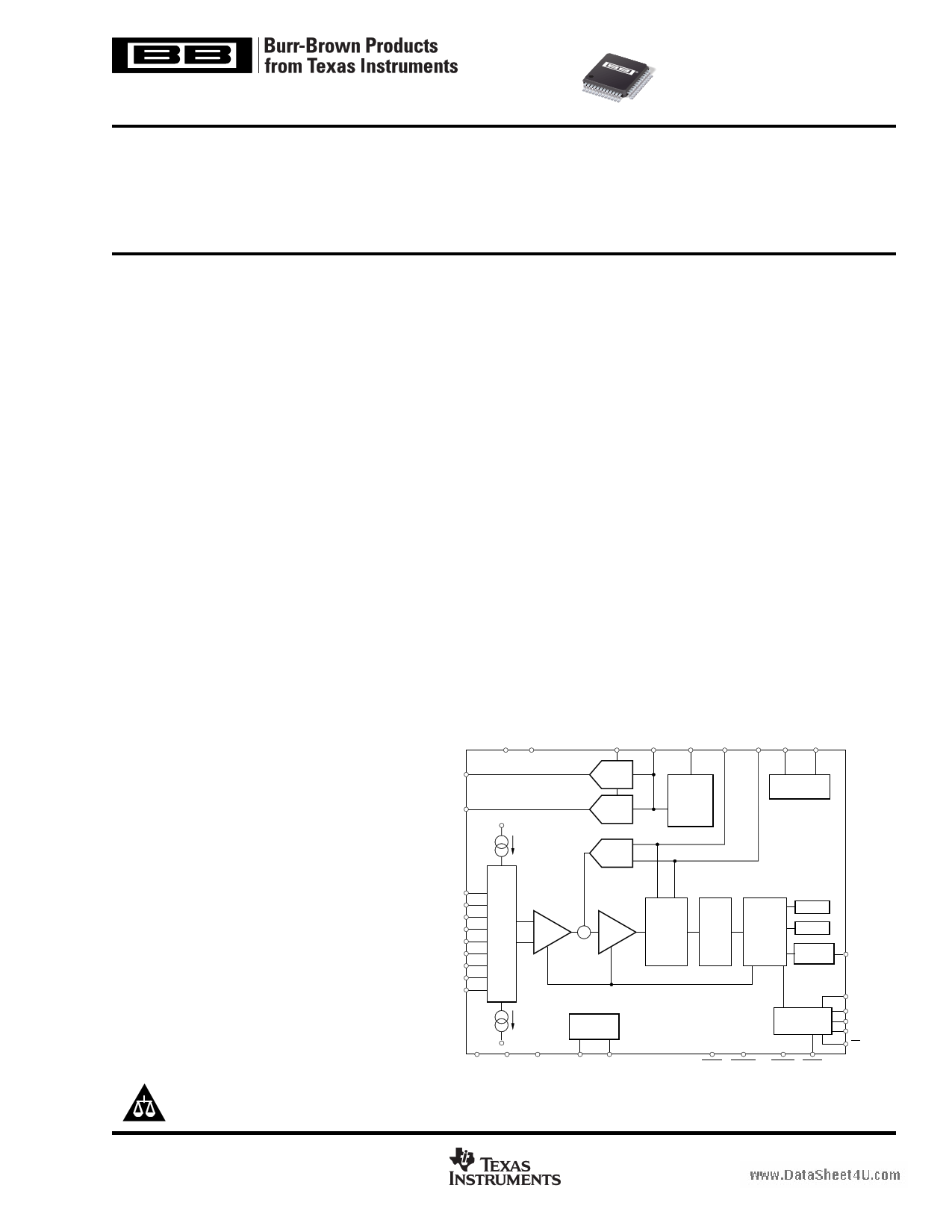
AGND AVDD
RDAC
VREFOUT
VRCAP
VREF+
VREF–
XIN
XOUT
APPLICATIONS
q INDUSTRIAL PROCESS CONTROL
q LIQUID /GAS CHROMATOGRAPHY
q BLOOD ANALYSIS
q SMART TRANSMITTERS
q PORTABLE INSTRUMENTATION
q WEIGHT SCALES
q PRESSURE TRANSDUCERS
SPI is a registered trademark of Motorola.
IDAC2
IDAC1
AVDD
2µA
8-Bit
IDAC
8-Bit
IDAC
Offset
DAC
1.25V or
2.5V
Reference
Clock Generator
AIN0
AIN1
AIN2
AIN3
AIN4
AIN5
AIN6
AIN7
AINCOM
IN+
MUX IN– BUF
2µA
AGND
DVDD DGND BUFEN
A = 1:128
+ PGA
Digital I/O
Interface
D0 ... D7
2nd-Order
Modulator
Program-
mable
Digital
Filter
Registers
Controller
RAM
4K Bytes
FLASH
Serial Interface
PDWN DSYNC RESET DRDY
WREN
POL
SCLK
DIN
DOUT
CS
Please be aware that an important notice concerning availability, standard warranty, and use in critical applications of
Texas Instruments semiconductor products and disclaimers thereto appears at the end of this data sheet.
PRODUCTION DATA information is current as of publication date.
Products conform to specifications per the terms of Texas Instruments
standard warranty. Production processing does not necessarily include
testing of all parameters.
www.ti.com
Copyright © 2001, Texas Instruments Incorporated
1 page 
www.DataShEeeLt4UE.coCmTRICAL CHARACTERISTICS: AVDD = 3V (Cont.)
All specifications TMIN to TMAX, AVDD = +3V, DVDD = +2.7V to 5.25V, fMOD = 19.2kHz, fOSC = 2.4576MHz, PGA = 1, Buffer ON, RDAC = 75kΩ, fDATA=10Hz,
VREF ≡ (REF IN+) – (REF IN–) = +1.25V unless otherwise specified.
ADS1218
PARAMETER
POWER-SUPPLY REQUIREMENTS
Power-Supply Voltage
Analog Current (IADC + IVREF + IDAC)
ADC Current (IADC)
VREF Current (IVREF)
IDAC Current (IDAC)
Digital Current
Power Dissipation
TEMPERATURE RANGE
Operating
Storage
CONDITIONS
AVDD
PDWN = 0, or SLEEP
PGA = 1, Buffer OFF
PGA = 128, Buffer OFF
PGA = 1, Buffer ON
PGA = 128, Buffer ON
Excludes Load Current
Normal Mode, DVDD = 3V
SLEEP Mode, DVDD = 3V
Read Data Continuous Mode, DVDD = 3V
PDWN = 0
PGA = 1, Buffer OFF, REFEN = 0,
IDACS OFF, DVDD = 3V
MIN
2.7
–40
–60
TYP
1
160
450
230
850
250
480
90
75
113
1
0.8
MAX
3.3
250
700
325
1325
375
675
200
1.4
+85
+100
UNITS
V
nA
µA
µA
µA
µA
µA
µA
µA
µA
µA
nA
mW
°C
°C
NOTES: (1) Calibration can minimize these errors. (2) ∆ VOUT is change in digital result. (3) 12pF switched capacitor at fSAMP clock frequency.
DIGITAL CHARACTERISTICS: TMIN to TMAX, DVDD = 2.7V to 5.25V
PARAMETER
CONDITIONS
MIN
TYP
MAX
UNITS
Digital Input/Output
Logic Family
Logic Level: VIH
VIL
VOH
VOL
Input Leakage: IIH
IIL
Master Clock Rate: fOSC(1)
Master Clock Period: tOSC(1)
IOH = 1mA
IOL = 1mA
VI = DVDD
VI = 0
1/fOSC
0.8 • DVDD
DGND
DVDD – 0.4
DGND
–10
1
200
CMOS
DVDD
0.2 • DVDD
DGND + 0.4
10
5
1000
V
V
V
V
µA
µA
MHz
ns
NOTE: (1) For FLASH E/W operations, the SPEED bit in the SETUP register must be set appropriately and the device operating frequency must be:
2.3MHz < FOSC < 4.13MHz.
FLASH CHARACTERISTICS: TMIN to TMAX, DVDD = 2.7V to 5.25V, unless otherwise specified.
PARAMETER
CONDITIONS
MIN TYP
MAX
Operating Current
Page Write
Page Read
Endurance
Data Retention
DVDD for Erase/Write
DVDD = 5V, During WR2F Command
DVDD = 3V, During WR2F Command
DVDD = 5V, During RF2R Command
DVDD = 3V, During RF2R Command
at 25°C
100
2.7
6.5
3.75
4.0
1.2
100,000
5.25
UNITS
mA
mA
mA
mA
E/W Cycles
Years
V
ADS1218
SBAS187
5
5 Page 
TYPICALwww.DataSheet4U.com CHARACTERISTICS (Cont.)
AVDD = +5V, DVDD = +5V, fOSC = 2.4576MHz, PGA = 1, RDAC = 150kΩ, fDATA = 10Hz, VREF ≡ (REF IN+) – (REF IN–) = +2.5V, unless otherwise specified.
1.00020
1.00016
1.00012
1.00008
1.00004
1.00000
0.99996
0.99992
0.99988
0.99984
0.99980
0.99976
–50
OFFSET DAC - GAIN vs TEMPERATURE
–30 –10 10 30 50
Temperature (°C)
70
90
1.000
1.000
0.999
0.999
0.998
0
IDAC ROUT vs VOUT
+25°C
+85°C
–40°C
1 234
VDD – VOUT (V)
5
1.01
IDAC NORMALIZED vs TEMPERATURE
1.005
1
0.995
0.99
0.985
–50 –30 –10 10 30 50 70 90
Temperature (°C)
3000
2000
1000
0
–1000
–2000
–3000
–4000
–5000
–6000
–50
IDAC MATCHING vs TEMPERATURE
–30 –10 10 30 50
Temperature (°C)
70
90
0.5
0.4
0.3
0.2
0.1
0
–0.1
–0.2
–0.3
–0.4
–0.5
0
IDAC DIFFERENTIAL NON-LINEARITY
RANGE = 1, RDAC = 150kΩ, VREF = 2.5V
32 64 96 128 160 192 224 255
IDAC Code
0.5
0.4
0.3
0.2
0.1
0
–0.1
–0.2
–0.3
–0.4
–0.5
0
IDAC INTEGRAL NON-LINEARITY
RANGE = 1, RDAC = 150kΩ, VREF = 2.5V
32 64 96 128 160 192 224 255
IDAC Code
ADS1218
SBAS187
11
11 Page | ||
| Páginas | Total 30 Páginas | |
| PDF Descargar | [ Datasheet ADS1218.PDF ] | |
Hoja de datos destacado
| Número de pieza | Descripción | Fabricantes |
| ADS1210 | 24-Bit ANALOG-TO-DIGITAL CONVERTER | Burr-Brown Corporation |
| ADS1210 | 24-Bit Analog-to-Digital Converter (Rev. B) | Texas Instruments |
| ADS1210P | 24-Bit ANALOG-TO-DIGITAL CONVERTER | Burr-Brown Corporation |
| ADS1210U | 24-Bit ANALOG-TO-DIGITAL CONVERTER | Burr-Brown Corporation |
| Número de pieza | Descripción | Fabricantes |
| SLA6805M | High Voltage 3 phase Motor Driver IC. |
Sanken |
| SDC1742 | 12- and 14-Bit Hybrid Synchro / Resolver-to-Digital Converters. |
Analog Devices |
|
DataSheet.es es una pagina web que funciona como un repositorio de manuales o hoja de datos de muchos de los productos más populares, |
| DataSheet.es | 2020 | Privacy Policy | Contacto | Buscar |