|
|
PDF KS0108B Data sheet ( Hoja de datos )
| Número de pieza | KS0108B | |
| Descripción | 64CH SEGMENT DRIVER | |
| Fabricantes | Samsung semiconductor | |
| Logotipo | ||
Hay una vista previa y un enlace de descarga de KS0108B (archivo pdf) en la parte inferior de esta página. Total 17 Páginas | ||
|
No Preview Available !
www.DataSheet4U.com
KS0108B
64CH SEGMENT DRIVER FOR DOT MATRIX LCD
INTRODUCTION
The KS0108B is a LCD driver LSl with 64 channel output
for dot matrix liquid crystal graphic display system. This
device consists of the display RAM, 64 bit data latch 64 bit
drivers and decoder logics. It has the internal display RAM
for storing the display data transferred from a 8 bit micro
controller and generates the dot matrix Iiquid crystal driv-
ing signals corresponding to stored data.The KS0108B
composed of the liquid crystal display system in combina-
tion with the KS0107B (64 common driver)
FEATURES
• Dot matrix LCD segment driver with 64 channel output
• Input and Output signal
- Input: 8 bit parallel display data
Control signal from MPU
Splitted bias voltage (V1R, V1L, V2R, V2L,
V3R. V3L, V4R, V4L)
- Output: 64 channel waveform for LCD driving.
• Display data is stored in display data RAM from MPU.
• Interface RAM
- Capacity: 512 bytes (4096 bits)
- RAM bit data: RAM bit data = 1:ON
RAM bit data- = 0:OFF
• Applicable LCD duty: 1/32~1/64
• LCD driving voltage: 8V~17V(VDD-VEE)
• Power supply voltage: + 5V±10%
Driver
COMMON
SEGMENT
KS0107B Other KS0108B
Controller
MPU
• High voltage CMOS process.
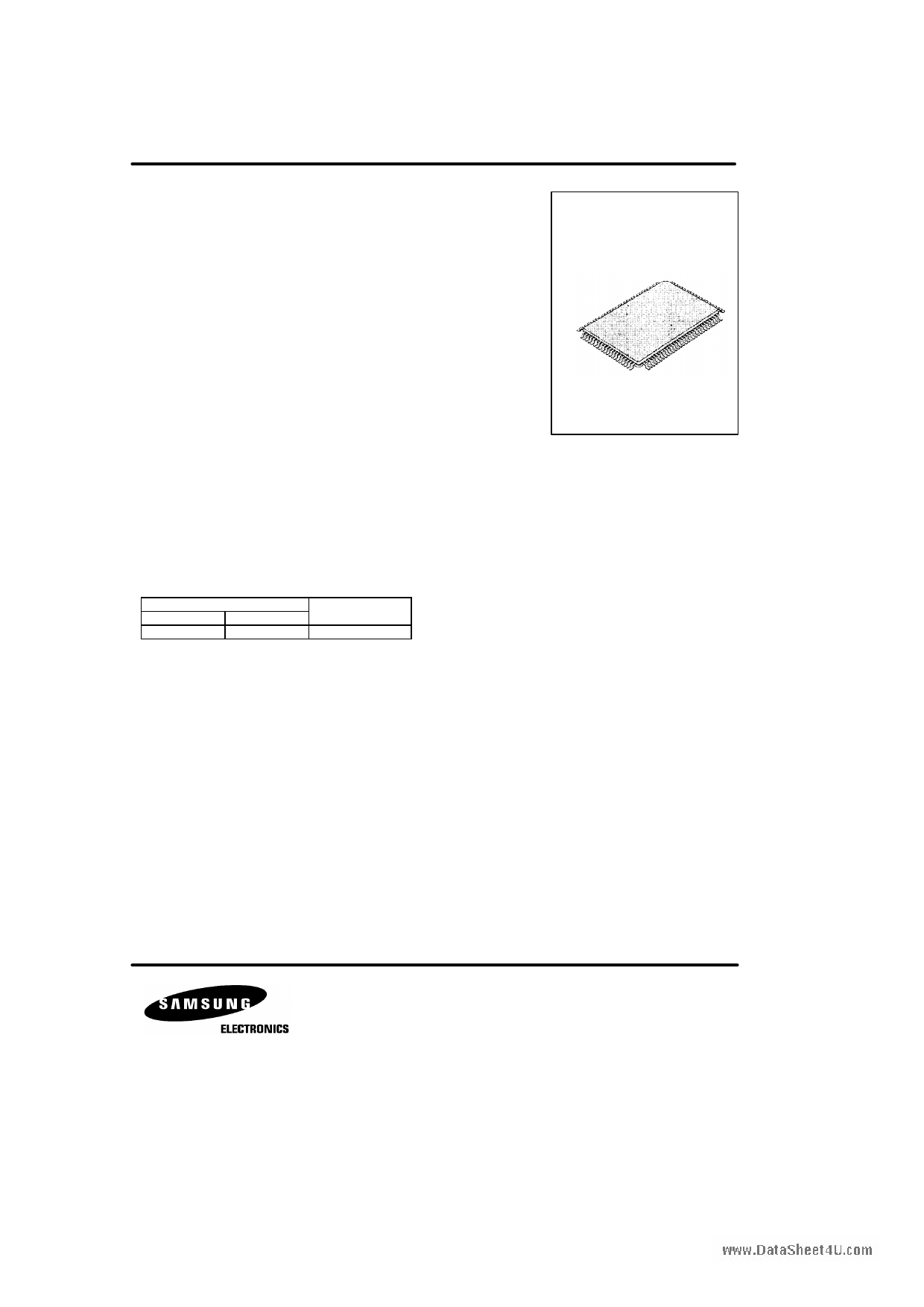
• 100QFP and bare chip available.
100 QFP
1 page 
www.DataSheet4U.com
KS0108B
64CH SEGMENT DRIVER FOR DOT MATRIX LCD
PIN DESCRIPTION(continued)
PIN (NO)
72~9
NAME
S1~S64
INPUT/OUTPUT
DESCRIPTION
Output
LCD Segment driver output.
Display RAM data 1:ON
Display RAM data 0:OFF
(Relation of display RAM data & M)
93 RSTB
87~89
NC
Input
M
DATA
Output Level
LL
H
HL
H
V2
V0
V3
V5
Reset signal.
When RSTB=L,
(1) ON/OFF register becomes set by 0. (display off)
(2) Display start line register becomes set by 0
(Z-address 0 set, display from line 0)
After releasing reset, this condition can be changed only by instruction.
No connection.(open)
MAXIMUM ABSOLUTE LIMIT
Characteristic
Symbol
Value
Unit
Operating Voltage
Supply Voltage
Driver Supply Voltage
Operating Temperature
VDD
VEE
VB
VLCD
TOPR
-0.3~+7.0
VDD-19.0~VDD+0.3
-0.3~VDD+0.3
VEE-0.3~VDD+0.3
-30~+85
V
V
V
V
°C
Storage Temperature
TSTG
-55~+125
°C
*1. Based on VSS=0V.
*2. Applies the same supply voltage to VEE1 and VEE2. VLCD=VDD-VEE.
*3. Applies to M, FRM, CL, RSTB, ADC, CLK1, CLK2, CS1B, CS2B, CS3, E, R/W, RS and DB0~DB7.
*4. Applies V0L(R), V2L(R), V3L(R) and V5L(R).
Voltage level: VDD≥V0L=VOR≥V2L=V2R≥V3L=V3R≥V5L=V5R≥VEE.
Note
*1
*4
*1,3
*2
5 Page 
www.DataSheet4U.com
KS0108B
64CH SEGMENT DRIVER FOR DOT MATRIX LCD
OPERATING PRINCIPLES & METHODS
1. I/O Buffer
Input buffer controls the status between the enable and disable of chip. Unless the CS1B to CS3 is in active mode, Input or
output of data and instruction does not execute. Therefore internal state is not change. But RSTB and ADC can operate
regardless CS1B-CS3.
2. Input register
Input register is provided to interface with MPU which is different operating frequency. Input register stores the data tempor-
arily before writing it into display RAM.
When CS1B to CS3 are in the active mode, R/W and RS select the input register. The data from MPU is written into input
register. Then Writing it into display RAM. Data latched for falling of the E signal and write automatically into the display data
RAM by internal operation.
3. Output register
Output register stores the data temporarily from display data RAM when CS1B, CS2B, CS3 is in active mode and R/W and
RS=H, stored data in display data RAM is latched in output register. When CS1B to CS3 is in active mode and R/W=H, RS=L,
status data (busy check) can read out.
To read the contents of display data RAM, twice access of read instruction is needed. In first access, data in display data RAM
is latched into output register. In second access, MPU can read data which is latched. That is, to read the data in display data
RAM, it needs dummy read. But status read is not needed dummy read.
RS R/W
LL
H
HL
H
Function
Instruction
Status read (busy check)
Data write (from input register to display data RAM)
Data read (from display data RAM to output register)
4. Reset
Reset can be initialized system by setting RSTB terminal at low level when turning power on, receiving instruction from MPU.
When RSTB becomes low, following procedure is occured.
1. Display off
2. Display start line register become set by 0.(Z-address 0)
While RSTB is low, any instruction except status read can be accepted. Reset status appers at DB4. After DB4 is low, any
instruction can be accepted.
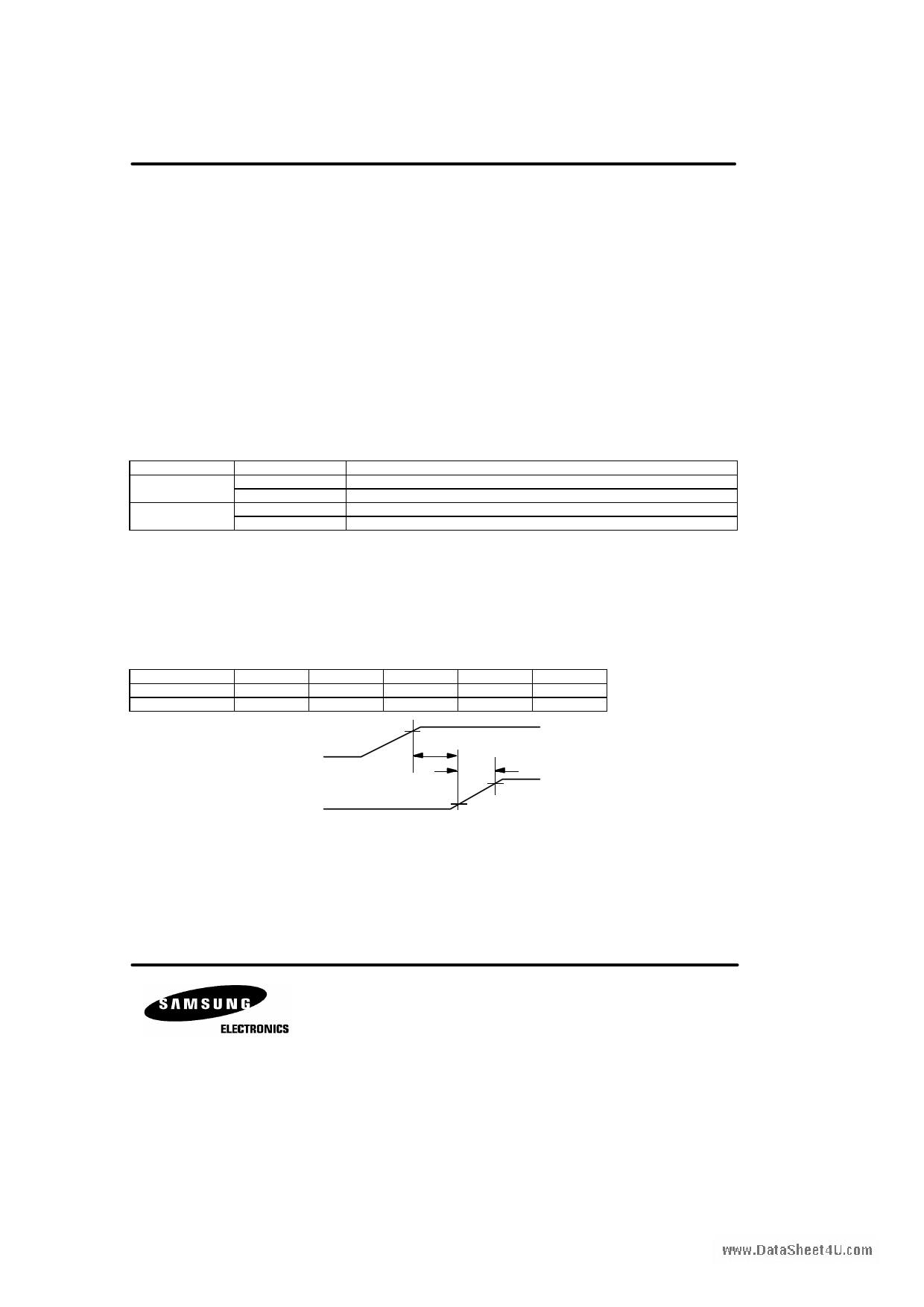
The Conditions of power supply at initial power up are shown in table 1.
Table 1. Power Supply Initial Conditions
Item
Symbol
Reset Time
Rise Time
tRS
tR
Min
1.0
-
Typ Max Unit
- - us
- 200 ns
VDD
RSTB
4.5[V]
tRS
tR
0.7VDD
0.3VDD
11 Page | ||
| Páginas | Total 17 Páginas | |
| PDF Descargar | [ Datasheet KS0108B.PDF ] | |
Hoja de datos destacado
| Número de pieza | Descripción | Fabricantes |
| KS0108 | 64CH SEGMENT DRIVER | Samsung semiconductor |
| KS0108 | KS0108 | ETC |
| KS0108B | 64CH SEGMENT DRIVER | Samsung semiconductor |
| Número de pieza | Descripción | Fabricantes |
| SLA6805M | High Voltage 3 phase Motor Driver IC. |
Sanken |
| SDC1742 | 12- and 14-Bit Hybrid Synchro / Resolver-to-Digital Converters. |
Analog Devices |
|
DataSheet.es es una pagina web que funciona como un repositorio de manuales o hoja de datos de muchos de los productos más populares, |
| DataSheet.es | 2020 | Privacy Policy | Contacto | Buscar |
