|
|
PDF KM29N040IT Data sheet ( Hoja de datos )
| Número de pieza | KM29N040IT | |
| Descripción | Flash Memory | |
| Fabricantes | Samsung Electronics | |
| Logotipo |  |
|
Hay una vista previa y un enlace de descarga de KM29N040IT (archivo pdf) en la parte inferior de esta página. Total 21 Páginas | ||
|
No Preview Available !
www.DataSheet4U.com
KM29N040T, KM29N040IT
Document Title
512K x 8 Bit NAND Flash Memory
Revision History
Revision No. History
0.0 Data Sheet 1997.
1.0 Data Sheet 1998.
1.1 Data Sheet 1998.
FLASH MEMORY
Draft Date
April 10th 1997
April 10th 1998
July 14th 1998
Remark
Final
The attached datasheets are prepared and approved by SAMSUNG Electronics. SAMSUNG Electronics CO., LTD. reserve the right to cha nge the
specifications. SAMSUNG Electronics will evaluate and reply to your requests and questions about device. If you have any questio ns, please contact the
SAMSUNG branch office near you.
1
1 page 
www.DataSheet4U.com
KM29N040T, KM29N040IT
FLASH MEMORY
PIN DESCRIPTION
Command Latch Enable(CLE)
The CLE input controls the path activation for commands sent to the command register. When active high, commands are latched
into the command register through the I/O ports on the rising edge of the WE signal.
Address Latch Enable(ALE)
The ALE input controls the path activation for address and input data to the internal address/data register. Addresses are latch ed on
the rising edge of WE with ALE high, and input data is latched when ALE is low.
Chip Enable(CE)
The CE input is the device selection control. When CE goes high during a read operation the device is returned to standby mode.
However, when the device is in the busy state during program or erase, CE high is ignored, and does not return the device to standby
mode.
Write Enable( WE)
The WE input controls writes to the I/O port. Commands, address and data are latched on the rising edge of the WE pulse.
Read Enable( RE)
The RE input is the serial data-out control, and when active drives the data onto the I/O bus. Data is valid t REA after the falling edge
of RE which also increments the internal column address counter by one.
I/O Port : I/O 0 ~ I/O7
The I/O pins are used to input command, address and data, and to output data during read operations. The I/O pins float to high- z
when the chip is deselected or when the outputs are disabled.
Write Protect( WP)
The WP pin provides inadvertent write/erase protection during power transitions. The internal high voltage generator is reset when
the WP pin is active low.
Ready/Busy(R/B)
The R/B output indicates the status of the device operation. When low, it indicates that a program, erase or random read operation is
in process and returns to high state upon completion. It is an open drain output and does not float to high-z condition when the chip
is deselected or when outputs are disabled.
5
5 Page 
www.DataSheet4U.com
KM29N040T, KM29N040IT
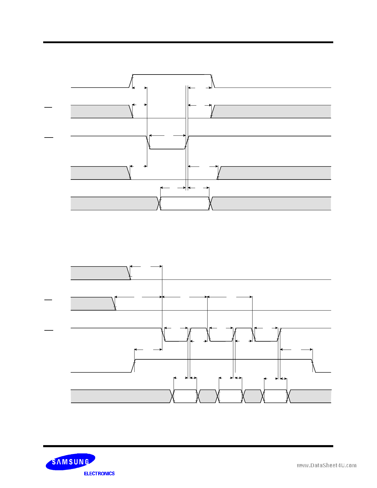
* Command Latch Cycle
CLE
CE
WE
ALE
I/O0~7
tCLS
tCS
tCLH
tCH
tWP
tALS
tALH
tDS tDH
Command
FLASH MEMORY
* Address Latch Cycle
CLE
CE
WE
ALE
I/O0~7
tCLS
tCS tWC tWC
tALS
tWP tWP tWP
tWH tWH
tALH
tDS tDH
A0~A7
tDS tDH
A8~A15
tDS tDH
A16~A18
11
11 Page | ||
| Páginas | Total 21 Páginas | |
| PDF Descargar | [ Datasheet KM29N040IT.PDF ] | |
Hoja de datos destacado
| Número de pieza | Descripción | Fabricantes |
| KM29N040IT | Flash Memory | Samsung Electronics |
| Número de pieza | Descripción | Fabricantes |
| SLA6805M | High Voltage 3 phase Motor Driver IC. |
Sanken |
| SDC1742 | 12- and 14-Bit Hybrid Synchro / Resolver-to-Digital Converters. |
Analog Devices |
|
DataSheet.es es una pagina web que funciona como un repositorio de manuales o hoja de datos de muchos de los productos más populares, |
| DataSheet.es | 2020 | Privacy Policy | Contacto | Buscar |
