|
|
PDF ICE2QS01 Data sheet ( Hoja de datos )
| Número de pieza | ICE2QS01 | |
| Descripción | Quasi-Resonant PWM Controller | |
| Fabricantes | Infineon Technologies | |
| Logotipo |  |
|
Hay una vista previa y un enlace de descarga de ICE2QS01 (archivo pdf) en la parte inferior de esta página. Total 17 Páginas | ||
|
No Preview Available !
www.DataSheet4U.com
Datasheet Version 2.0, December 2006
ICE2QS01
Quasi-resonant PWM
Controller
Power Management & Supply
Never stop thinking.
1 page 
www.DataSheet4U.com
Quasi-Resonant PWM Controller
ICE2QS01
Pin Configuration and Functionality
1
1.1
Pin
1
2
3
4, 5
6
7
8
1.2
Pin Configuration and Functionality
Pin Configuration
Symbol Function
ZC
REG
CS
HV
OUT
Zero Crossing
Regulation
Primary Current Sensing
High Voltage input
gate driver output
REG (Regulation)
Normally, an external capacitor is connected to this pin
for a smooth voltage Vreg. Internally, this pin is
connected to the PWM signal generator for switch-off
determination (together with the current sensing
signal), the digital signal processing for the frequency
reduction with decreasing load during normal
operation, and the burst mode controller for entering
burst mode operation determination and burst ratio
control during burst mode operation. Additionally, the
open-loop / over-load protection is implemented by
monitoring the voltage at this pin.
VCC
GND
IC supply voltage
Common ground
Package PG-DIP-8
CS (Current Sensing)
This pin is connected to the shunt resistor for the
primary current sensing, externally, and the PWM
signal generator for switch-off determination (together
with the regulation voltage), internally. Moreover, short-
winding protection is realised by monitoring the voltage
Vcs during on-time of the main power switch.
ZC 1
REG
2
CS 3
8
GND
HV (High Voltage)
The pin HV is connected to the bus voltage, externally,
and to the power cell, internally. The current through
7
VCC
this pin pre-charges the VCC capacitor once the supply
bus voltage is applied. Additionally, the current through
this pin supplies the IC in case that the output voltage
is lowered during active burst mode operation, or
6
OUT
during latch-off mode.
HV 4
5 HV
OUT (Gate drive output)
This output signal drives the external main power
switch, which is a power MOSFET in most case.
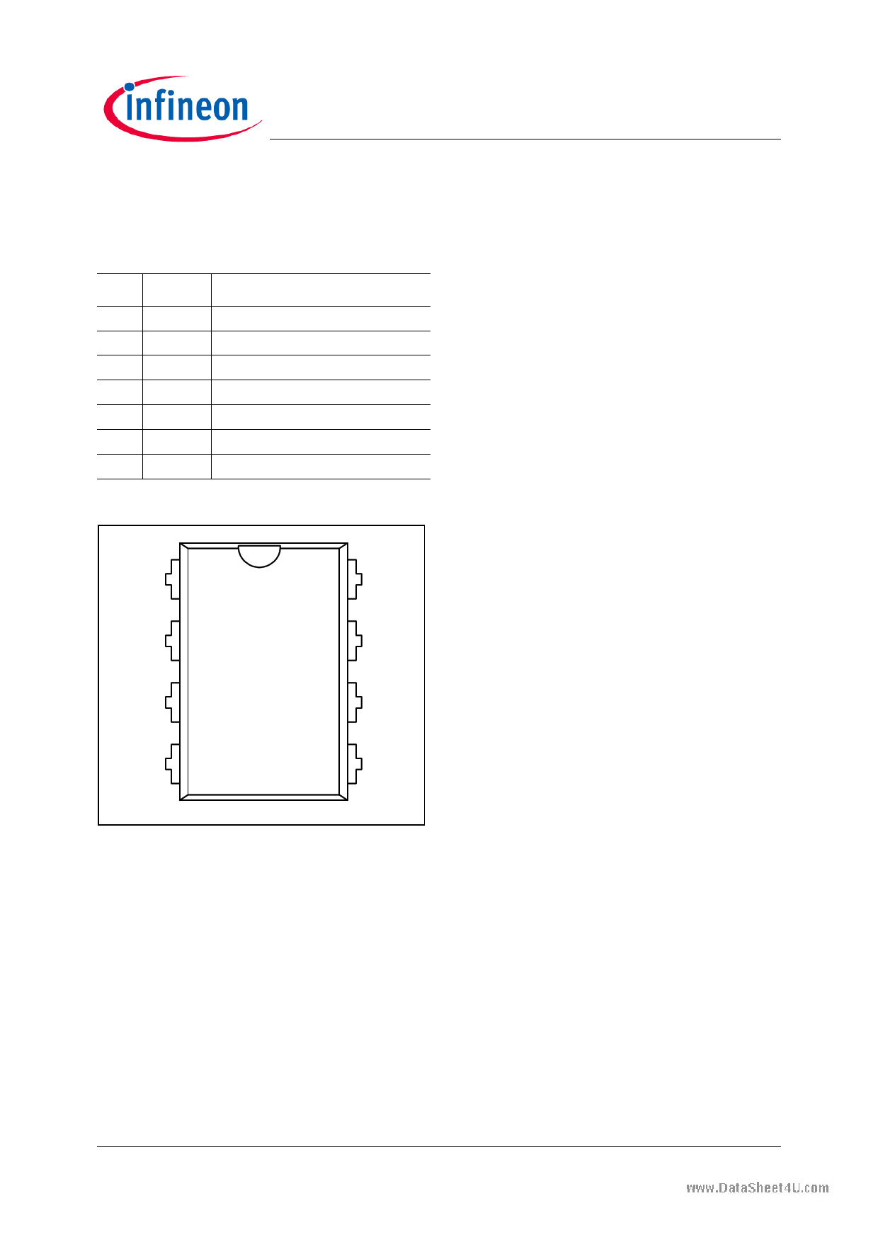
Figure 1 Pin Configuration PG-DIP-8(top view)
1.3 Pin Functionality
ZC (Zero Crossing)
At this pin, the voltage from the auxiliary winding after
a time delay circuit is applied. Internally, this pin is
connected to the zero-crossing detector for switch-on
determination. Additionally, the output overvoltage
detection is realized by comparing the voltage Vzc with
an internal preset threshold.
VCC (Power supply)
This is the IC power supply pin. Externally, this pin is
connected to the VCC capacitor, which is supplied by
the inside power cell during VCC charge-up, burst
mode operation at lowered output voltage or during
latched-off of the IC, and the auxiliary winding during
normal operation or burst mode operation with high
enough voltage across the auxiliary winding. Based on
this voltage, the VCC under- or over-voltage protection
are implemented.
GND (Ground)
This is the common ground of the controller.
Version 2.0
5 December 2006
5 Page 
www.DataSheet4U.com
3.5 Protection Functions
The IC provides full protection functions. The following
table summarizes these protection functions.
Table 2 Protection features
VCC Overvoltage
Auto Restart Mode
VCC Undervoltage
Auto Restart Mode
Overload/Open Loop
Auto Restart Mode
Output Overvoltage
Latched Off Mode
Short Winding
Latched Off Mode
During operation, the VCC voltage is continuously
monitored. In case of an under- or an over-voltage, the
IC is reset and the main power switch is then kept off.
After the VCC voltage falls below the threshold
VVCCUVP, the power cell is activated. The VCC capacitor
is then charged up. Once the voltage exceeds the
threshold VVCCon, the IC begins to operate with a new
soft-start.
In case of open control loop or output over load, the
regulation voltage will be pulled up . After a blanking
time of 24ms, the IC enters auto-restart mode. The
blanking time here enables the converter to provide a
high power in case the increase in VREG is due to a
sudden load increase. During off-time of the power
switch, the voltage at the zero-crossing pin is
monitored for output over-voltage detection. If the
voltage is higher than the preset threshold vOPOVP, the
IC is latched off after the preset blanking time.
If the voltage at the current sensing pin is higher than
the preset threshold vcsSW during on-time of the power
switch, the IC is latched off. This is short-winding
protection.
During latch-off protection mode, the power cell is
activated and it keeps the VCC voltage at the level of
VVCCBL.
Quasi-Resonant PWM Controller
ICE2QS01
Functional Description
Version 2.0
11 December 2006
11 Page | ||
| Páginas | Total 17 Páginas | |
| PDF Descargar | [ Datasheet ICE2QS01.PDF ] | |
Hoja de datos destacado
| Número de pieza | Descripción | Fabricantes |
| ICE2QS01 | Quasi-Resonant PWM Controller | Infineon Technologies |
| ICE2QS01-160W | 160W SMPS Evaluation Board | Infineon Technologies |
| ICE2QS03 | Quasi-Resonant PWM Controller | Infineon Technologies |
| ICE2QS03G | Quasi-Resonant PWM controller | Infineon |
| Número de pieza | Descripción | Fabricantes |
| SLA6805M | High Voltage 3 phase Motor Driver IC. |
Sanken |
| SDC1742 | 12- and 14-Bit Hybrid Synchro / Resolver-to-Digital Converters. |
Analog Devices |
|
DataSheet.es es una pagina web que funciona como un repositorio de manuales o hoja de datos de muchos de los productos más populares, |
| DataSheet.es | 2020 | Privacy Policy | Contacto | Buscar |
