|
|
|
PDF ICS43002I-41 Data sheet ( Hoja de datos )
| Número de pieza | ICS43002I-41 | |
| Descripción | FEMTOCLOCKS-TM VCXO BASED SONET/SDH JITTER ATTENUATOR | |
| Fabricantes | ICS | |
| Logotipo | ||
Hay una vista previa y un enlace de descarga de ICS43002I-41 (archivo pdf) en la parte inferior de esta página. Total 21 Páginas | ||
|
No Preview Available !
www.DataSheet4U.com
Integrated
Circuit
Systems, Inc.
PRELIMINARY
ICS843002I-41
700MHZ, FEMTOCLOCKS™ VCXO BASED
SONET/SDH JITTER ATTENUATOR
GENERAL DESCRIPTION
ICS
The ICS843002I-41 is a member of the
HiperClockS™ family of high performance clock
HiPerClockS™ solutions from ICS. The ICS843002I-41 is a PLL
based synchronous clock generator that is
optimized for SONET/SDH line card applications
where jitter attenuation and frequency translation is needed.
The device contains two internal PLL stages that are cascaded
in series. The first PLL stage uses a VCXO which is optimized
to provide reference clock jitter attenuation and to be jitter
tolerant, and to provide a stable reference clock for the 2nd
PLL stage (typically 19.44MHz). The second PLL stage
provides additional frequency multiplication (x32), and it
maintains low output jitter by using a low phase noise
FemtoClock™ VCO. PLL multiplication ratios are selected
from internal lookup tables using device input selection pins.
The device performance and the PLL multiplication ratios are
optimized to support non-FEC (non-Forward Error Correction)
SONET/SDH applications with rates up to OC-48 (SONET)
or STM-16 (SDH). The VCXO requires the use of an external,
inexpensive pullable crystal. VCXO PLL uses external passive
loop filter components which are used to optimize the PLL
loop bandwidth and damping characteristics for the given
line card application.
FEATURES
• (2) Differential LVPECL outputs
• Selectable CLKx, nCLKx differential input pairs
• CLKx, nCLKx pairs can accept the following differential
input levels: LVPECL, LVDS, LVHSTL, SSTL, HCSL or
single-ended LVCMOS or LVTTL levels
• Maximum output frequency: 700MHz
• FemtoClock VCO frequency range: 560MHz - 700MHz
• RMS phase jitter @ 155.52MHz, using a 19.44MHz crystal
(12kHz to 20MHz): 0.81ps (typical)
• Full 3.3V or mixed 3.3V core/2.5V output supply voltage
• -40°C to 85°C ambient operating temperature
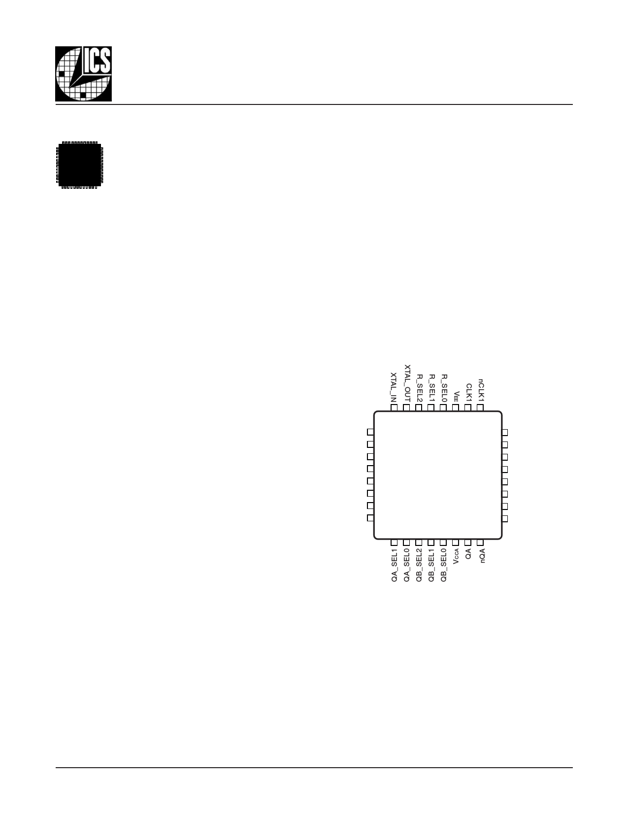
PIN ASSIGNMENT
The ICS843002I-41 includes two clock input ports. Each one
can accept either a single-ended or differential input. Each
input port also includes an activity detector circuit, which
reports input clock activity through the LOR0 and LOR1 logic
output pins. The two input ports feed an input selection mux.
“Hitless switching” is accomplished through proper filter
tuning. Jitter transfer and wander characteristics are
influenced by loop filter tuning, and phase transient
performance is influenced by both loop filter tuning and
alignment error between the two reference clocks.
Typical ICS843002I-41 configuration in SONET/SDH Systems:
• VCXO 19.44MHz crystal
• Loop bandwidth: 50Hz - 250Hz
• Input Reference clock frequency selections:
19.44MHz, 38.88MHz, 77.76MHz, 155.52MHz,
311.04MHz, 622.08MHz
• Output clock frequency selections:
19.44MHz, 77.76MHz, 155.52MHz, 311.04MHz,
622.08MHz, Hi-Z
LF1
LF0
ISET
VCC
CLK0
nCLK0
CLK_SEL
QA_SEL2
32 31 30 29 28 27 26 25
1 24
2 23
3 22
4 21
5 20
6 19
7 18
8 17
9 10 11 12 13 14 15 16
LOR0
LOR1
nc
VCCO_LVCMOS
VCCO_LVPECL
nQB
QB
VEE
ICS843002I-41
32-Lead VFQFN
5mm x 5mm x 0.75mm package body
K Package
Top View
The Preliminary Information presented herein represents a product in prototyping or pre-production. The noted characteristics are based on initial
product characterization. Integrated Circuit Systems, Incorporated (ICS) reserves the right to change any circuitry or specifications without notice.
843002AKI-41
www.icst.com/products/hiperclocks.html
REV. A JUNE 1, 2005
1
1 page 
Integrated
Circuit
Systems, Inc.
PRELIMINARY
ICS843002I-41
700MHZ, FEMTOCLOCKS™ VCXO BASED
SONET/SDH JITTER ATTENUATOR
ABSOLUTE MAXIMUM RATINGS
Supply Voltage, VCC
Inputs, VI
Outputs, VO (LVCMOS)
Outputs, IO (LVPECL)
Continuous Current
Surge Current
4.6V
-0.5V to VCC + 0.5V
-0.5V to VCCO + 0.5V
50mA
100mA
Package Thermal Impedance, θJA 34.8°C/W (0 lfpm)
Storage Temperature, TSTG
-65°C to 150°C
NOTE: Stresses beyond those listed under Absolute
Maximum Ratings may cause permanent damage to the
device.These ratings are stress specifications only. Functional
operation of product at these conditions or any conditions be-
yond those listed in the DC Characteristics or AC Character-
istics is not implied. Exposure to absolute maximum rating
conditions for extended periods may affect product reliability.
TABLE
4A.
POWER
SUPPLY
DC
CHARACTERISTICS,
V
CC
=
V=
CCA
3.3V±5%,
V,
CCO_LVCMOS
V
CCO_LVPECL
=
3.3V±5%
OR
2.5V±5%,
TA = -40°C TO 85°C
Symbol
VCC
VCCA
V
CCO_LVCMOS,
VCCO_LVPECL
IEE
ICCA
Parameter
Core Supply Voltage
Analog Supply Voltage
Output Supply Voltage
Power Supply Current
Analog Supply Current
Test Conditions
Minimum
3.135
3.135
3.135
2.375
Typical
3.3
3.3
3.3
2.5
175
10
Maximum
3.465
3.465
3.465
2.625
Units
V
V
V
V
mA
mA
TABLE 4B. LVCMOS / LVTTL DC CHARACTERISTICS, VCC = VCCA = 3.3V±5%, VCCO_LVCMOS = 3.3V±5% OR 2.5V±5%,
TA = -40°C TO 85°C
Symbol Parameter
Test Conditions Minimum Typical Maximum Units
VIH Input High Voltage
VIL Input Low Voltage
2
VCC + 0.3
V
-0.3 0.8 V
I
IH
CLK_SEL, QA_SEL2,
Input
QB_SEL2, R_SEL0:R_SEL2
High Current
VCC = VIN = 3.465V
150 µA
QA_SEL0:1, QB_SEL0:1
VCC = VIN = 3.465V
5 µA
CLK_SEL, QA_SEL2,
V = 3.465V,
CC
IIL
Input
QB_SEL2, R_SEL0:R_SEL2
Low Current
QA_SEL0:1, QB_SEL0:1
VIN = 0V
VCC = 3.465V,
VIN = 0V
-5
-150
µA
µA
VOH
Output
High Voltage
LOR0, LOR1; NOTE 1
VOL
Output
Low Voltage
LOR0, LOR1; NOTE 1
VCCO_LVCMOS = 3.3V
VCCO_LVCMOS = 2.5V
VCCO_LVCMOS = 3.3V or
2.5V
2.6
1.8
V
V
0.5 V
NOTE
1:
Outputs
terminated
with
50Ω
to V /2
CCO_LVCMOS
.See
Parameter
Measurement
Information
Section,
“Output Load Test Circuit”.
843002AKI-41
www.icst.com/products/hiperclocks.html
5
REV. A JUNE 1, 2005
5 Page 
Integrated
Circuit
Systems, Inc.
PRELIMINARY
ICS843002I-41
700MHZ, FEMTOCLOCKS™ VCXO BASED
SONET/SDH JITTER ATTENUATOR
EXTERNAL VCXO PLL COMPONENTS
In general, the loop damping factor should be 0.7 or greater to
ensure output stability. A higher damping factor will create less
peaking in the passband. A higher damping factor may also
increase lock time and output clock jitter when there is excess
digital noise in the system application, due to the reduced ability
of the PLL to respond to and therefore compensate for phase
noise ingress.
LF1 1
32 31
LF0 2
CP RS ISET 3
CS
CP establishes a second pole in the VCXO PLL loop filter. For
higher damping factors (> 1), calculate the value of CP based on
a C value that would be used for a damping factor of 1.This will
S
minimize baseband peaking and loop instability that can lead to
output jitter.
CP also dampens VCXO PLL input voltage modulation by the
charge pump correction pulses. A CP value that is too low will
result in increased output phase noise at the phase detector
frequency due to this. In extreme cases where input jitter is high,
charge pump current is high, and CP is too small, the VCXO PLL
input voltage can hit the supply or ground rail resulting in non-
linear loop response.
The best way to set the value of CP is to use the filter response
software under development from ICS (please refer to the
following section). CP should be increased in value until it just
starts affecting the passband peak.
RSET LOOP FILTER RESPONSE SOFTWARE
Online tools to calculate loop filter response (coming soon) at
www.icst.com. Contact your local sales representative if a tool
cannot be found for this product.
The external crystal devices and loop filter components should
be kept close to the device. Loop filter and crystal PCB
connection traces should be kept short and well separated from
each other and from other signal traces. Other signal traces
should not run underneath the device, the loop filter or crystal
components.
NOTES ON SETTING THE VALUE OF CP
As another general rule, the following relationship should be
maintained between components CS and CP in the loop filter:
CP
=
CS
20
NOTES ON EXTERNAL CRYSTAL LOAD CAPACITORS
In the loop filter schematic diagram, capacitors are shown be-
tween pins 32 to ground and between pins 31 to ground. These
are optional crystal load capacitors which can be used to cen-
ter tune the external pullable crystal (the crystal frequency can
only be lowered by adding capacitance, it cannot be raised).
Note that the addition of external load capacitors will decrease
the crystal pull range and the Kvco value.
LOSS OF REFERENCE INDICATOR (LOR0 AND LOR1) OUTPUT PINS.
The LOR0 and LOR1 pins are controlled by the internal clock as an “edge”). The LOR output will otherwise be low. The
activity monitor circuits. The clock activity monitor circuits are activity monitor does not flag excessive reference transitions in
clocked by the VCXO PLL phase detector feedback clock.
The LOR output is asserted high if there are three consecutive
feedback clock edges without any reference clock edges (in
an phase detector observation interval as an error.The monitor
only distinguishes between transitions occurring and no transi-
tions occurring.
both cases, either a negative or positive transition is counted
843002AKI-41
www.icst.com/products/hiperclocks.html
11
REV. A JUNE 1, 2005
11 Page | ||
| Páginas | Total 21 Páginas | |
| PDF Descargar | [ Datasheet ICS43002I-41.PDF ] | |
Hoja de datos destacado
| Número de pieza | Descripción | Fabricantes |
| ICS43002I-40 | FEMTOCLOCKS-TM VCXO BASED SONET/SDH JITTER ATTENUATOR | ICS |
| ICS43002I-41 | FEMTOCLOCKS-TM VCXO BASED SONET/SDH JITTER ATTENUATOR | ICS |
| Número de pieza | Descripción | Fabricantes |
| SLA6805M | High Voltage 3 phase Motor Driver IC. |
Sanken |
| SDC1742 | 12- and 14-Bit Hybrid Synchro / Resolver-to-Digital Converters. |
Analog Devices |
|
DataSheet.es es una pagina web que funciona como un repositorio de manuales o hoja de datos de muchos de los productos más populares, |
| DataSheet.es | 2020 | Privacy Policy | Contacto | Buscar |