|
|
|
PDF DG409L Data sheet ( Hoja de datos )
| Número de pieza | DG409L | |
| Descripción | (DG408L / DG409L) Precision 8-Ch/Dual 4-Ch Low Voltage Analog Multiplexers | |
| Fabricantes | Vishay Siliconix | |
| Logotipo | ||
Hay una vista previa y un enlace de descarga de DG409L (archivo pdf) en la parte inferior de esta página. Total 16 Páginas | ||
|
No Preview Available !
www.vishay.com
DG408L, DG409L
Vishay Siliconix
Precision 8-Ch / Dual 4-Ch Low Voltage Analog Multiplexers
DESCRIPTION
The DG408L, DG409L are low voltage pin-for-pin
compatible companion devices to the industry standard
DG408, DG409 with improved performance.
Using BiCMOS wafer fabrication technology allows the
DG408L, DG409L to operate on single and dual supplies.
Single supply voltage ranges from 3 V to 12 V while dual
supply operation is recommended with ± 3 V to ± 6 V.
The DG408L is an 8 channel single-ended analog
multiplexer designed to connect one of eight inputs to a
common output as determined by a 3 bit binary address (A0,
A1, A2). The DG409L is a dual 4 channel differential analog
multiplexer designed to connect one of four differential
inputs to a common dual output as determined by its 2 bit
binary address (A0, A1). Break-before-make switching action
to protect against momentary crosstalk between adjacent
channels.
The DG408L, DG409L provides lower on-resistance, faster
switching time, lower leakage, less power consumption, and
higher off-isolation than the DG408, DG409.
FEATURES
• Pin-for-pin compatibility with DG408, DG409
• 2.7 V to 12 V single supply or ± 3 V to ± 6 V dual
supply operation
• Lower on-resistance: RDS(on) - 17 typ.
• Fast switching: tON - 38 ns, tOFF - 18 ns
• Break-before-make guaranteed
• Low leakage: IS(OFF) - 0.2 nA max.
• Low charge injection: 1 pC
Available
Available
Available
• TTL, CMOS, LV logic (3 V) compatible
• 82 dB off-isolation at 1 MHz
• 2000 V ESD protection (HBM)
• Material categorization: for definitions of compliance
please see www.vishay.com/doc?99912
Note
* This datasheet provides information about parts that are
RoHS-compliant and / or parts that are non-RoHS-compliant. For
example, parts with lead (Pb) terminations are not RoHS-compliant.
Please see the information / tables in this datasheet for details.
BENEFITS
• High accuracy
• Single and dual power rail capacity
• Wide operating voltage range
• Simple logic interface
APPLICATIONS
• Data acquisition systems
• Battery operated equipment
• Portable test equipment
• Sample and hold circuits
• Communication systems
• SDSL, DSLAM
• Audio and video signal routing
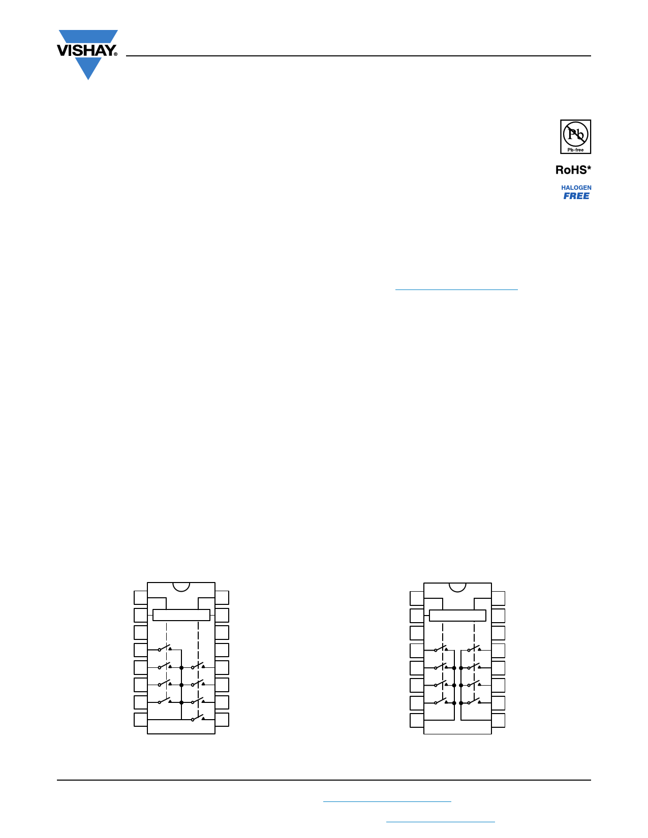
FUNCTIONAL BLOCK DIAGRAMS AND PIN CONFIGURATIONS
DG408L
Dual-In- Line, SOIC, and TSSOP
DG409L
Dual-In- Line, SOIC, and TSSOP
A0 1
16 A1
EN 2 Decoders/Drivers 15 A2
V-
3
GND
14
S1 4
V+
13
S2 5
12 S5
S3 6
11 S6
S4 7
10 S7
D
8
9 S8
Top View
A0 1
16 A1
EN 2 Decoders/Drivers 15 GND
V-
3
V+
14
S1a 4
S2a 5
13 S1b
12 S2b
S3a 6
11 S3b
S4a 7
10 S4b
Da 8
9 Db
Top View
S16-0276-Rev. J, 22-Feb-16
1
Document Number: 71342
For technical questions, contact: [email protected]
THIS DOCUMENT IS SUBJECT TO CHANGE WITHOUT NOTICE. THE PRODUCTS DESCRIBED HEREIN AND THIS DOCUMENT
ARE SUBJECT TO SPECIFIC DISCLAIMERS, SET FORTH AT www.vishay.com/doc?91000
1 page 
www.vishay.com
DG408L, DG409L
Vishay Siliconix
SPECIFICATIONS (Single Supply 5 V)
PARAMETER
Analog Switch
Analog Signal Range e
Drain-Source
On-Resistance
RDS(on) Matching Between
Channels g
On-Resistance Flatness i
Switch Off Leakage
Current a
SYMBOL
TEST CONDITIONS
UNLESS OTHERWISE
SPECIFIED
V+ = 5 V, ± 10 %, V- = 0 V
VEN = 0.6 V or 2.4 V f
TEMP. b
VANALOG
RDS(on)
V+ = 4.5 V, VD or VS = 1 V or 3.5 V,
IS = 5 mA
Full
Room
Full
RDS
RFLAT(on)
IS(off)
ID(off)
V+ = 4.5 V, VD = 1 V or 3.5 V,
IS = 5 mA
V+ = 5.5 V, VS = 1 V or 4 V,
VD = 4 V or 1 V
Room
Room
Room
Full
Room
Full
TYP. d
-
35
-
1.5
-
-
-
-
-
A SUFFIX
D SUFFIX
-55 °C to +125 °C -40 °C to +85 °C
MIN. c MAX. c MIN. c MAX. c
0505
- 49 - 40
- 62 - 62
-3-3
-4-4
-1 1 -1 1
-15 15 -10 10
-1 1 -1 1
-15 15 -10 10
UNIT
V
nA
Channel On Leakage
Current a
ID(on)
V+ = 5.5 V, VD = VS = 1 V or 4 V, Room
sequence each switch on
Full
-
-
-1 1 -1 1
-15 15 -10 10
Digital Control
Logic High Input Voltage
Logic Low Input Voltage
Input Current a
Dynamic Characteristics
VINH
VINL
IIN
V+ = 5 V
VAX = VEN = 2.4 V or 0.6 V
Full
Full
Full
- 2.4 - 2.4 -
V
- - 0.6 - 0.6
- -1.5 1.5 -1 1 μA
Transition Time e
tTRANS
VS1 = 3.5 V, VS8 = 0 V, (DG408L)
VS1b = 3.5 V, VS4b = 0 V, (DG409L)
see figure 2
Room
Full
44
-
- 125 - 125
- 138 - 135
Break-Before-Make Time e tOPEN
VS(all) = VDA = 3.5 V,
Room 17
1
-
1
-
see figure 4
Full - - - - - ns
Room 43 - 60 - 60
Enable Turn-On Time e
tON(EN) VAX = 0 V, VS1 = 3.5 V (DG408L)
Full
-
- 70 - 65
Enable Turn-Off Time e
tOFF(EN)
VAX = 0 V, VS1b = 3.5 V (DG409L)
see figure 3
Room
Full
26
-
-
-
45
60
-
-
45
50
Charge Injection e
Q
CL = 1 nF, RGEN = 0 ,
VGEN = 0 V
Room
-1
-
-
-
- pC
Off Isolation e, h
Crosstalk e
OIRR
Room -70
-
-
-
-
XTALK
f = 100 kHz, RL = 1 k
Room -80
-
-
-
dB
-
Source Off Capacitance e CS(off) f = 1 MHz, VS = 0 V, VEN = 0 V Room
8
-
-
-
-
Drain Off Capacitance e
CD(off) f = 1 MHz, VD = 0 V, VEN = 0 V Room
21
-
-
-
- pF
Drain On Capacitance e
CD(on) f = 1 MHz, VD = 0 V, VEN = 2.4 V Room
32
-
-
-
-
Notes
a. Leakage parameters are guaranteed by worst case test condition and not subject to production test.
b. Room = 25 °C, full = as determined by the operating temperature suffix.
c. The algebraic convention whereby the most negative value is a minimum and the most positive a maximum, is used in this data sheet.
d. Typical values are for DESIGN AID ONLY, not guaranteed nor subject to production testing.
e. Guaranteed by design, not subject to production test.
f. VIN = input voltage to perform proper function.
g. RDS(on) = RDS(on) max. - RDS(on) min.
h. Worst case isolation occurs on channel 4 do to proximity to the drain pin.
i. RDS(on) flatness is measured as the difference between the minimum and maximum measured values across a defined Analog signal.
S16-0276-Rev. J, 22-Feb-16
5
Document Number: 71342
For technical questions, contact: [email protected]
THIS DOCUMENT IS SUBJECT TO CHANGE WITHOUT NOTICE. THE PRODUCTS DESCRIBED HEREIN AND THIS DOCUMENT
ARE SUBJECT TO SPECIFIC DISCLAIMERS, SET FORTH AT www.vishay.com/doc?91000
5 Page 
www.vishay.com
TEST CIRCUITS
DG408L, DG409L
Vishay Siliconix
V+
Rg
Vg
Channel
Select
V+
SX
EN
A0
A1
A2
GND
D
V-
V-
VO
CL
1 nF
Logic
Input
3V
0V
OFF
ON
OFF
Switch
Output
VO
VO is the measured voltage due to charge transfer
error Q, when the channel turns off.
Q = CL x VO
Fig. 5 - Charge Injection
V+
V+
VS
Rg = 50
VIN
SX V+
S8
A0
A1
A2
GND
EN
D
V-
VO
RL
50
V-
Off Isolation = 20 log
VOUT
VIN
Fig. 6 - Off Isolation
VIN S1
VS SX
V+
Rg = 50
S8
A0
A1
A2
GND
EN
D
V-
VO
RL
50
V-
Crosstalk = 20 log
Fig. 7 - Crosstalk
VOUT
VIN
V+
VS
Rg = 50
V+
S1
A0
A1
A2
GND
EN
D
V-
VO
RL
50
V-
Insertion Loss = 20 log
VOUT
VIN
Fig. 8 - Insertion Loss
Channel
Select
V+
V+
A2
A1
A0
GND EN
S1
S8
D
V-
V-
Meter
HP4192A
Impedance
Analyzer
or Equivalent
f = 1 MHz
Fig. 9 - Source Drain Capacitance
Vishay Siliconix maintains worldwide manufacturing capability. Products may be manufactured at one of several qualified locations. Reliability data for Silicon
Technology and Package Reliability represent a composite of all qualified locations. For related documents such as package/tape drawings, part marking, and
reliability data, see www.vishay.com/ppg?71342.
S16-0276-Rev. J, 22-Feb-16
11
Document Number: 71342
For technical questions, contact: [email protected]
THIS DOCUMENT IS SUBJECT TO CHANGE WITHOUT NOTICE. THE PRODUCTS DESCRIBED HEREIN AND THIS DOCUMENT
ARE SUBJECT TO SPECIFIC DISCLAIMERS, SET FORTH AT www.vishay.com/doc?91000
11 Page | ||
| Páginas | Total 16 Páginas | |
| PDF Descargar | [ Datasheet DG409L.PDF ] | |
Hoja de datos destacado
| Número de pieza | Descripción | Fabricantes |
| DG409 | Single 8-Channel/Differential 4-Channel / CMOS Analog Multiplexers | Intersil Corporation |
| DG409 | 8-Ch/Dual 4-Ch High-Performance CMOS Analog Multiplexers | Vishay Siliconix |
| DG409 | (DG408 / DG409) CMOS Analog Multiplexers | Maxim Integrated Products |
| DG409L | (DG408L / DG409L) Precision 8-Ch/Dual 4-Ch Low Voltage Analog Multiplexers | Vishay Siliconix |
| Número de pieza | Descripción | Fabricantes |
| SLA6805M | High Voltage 3 phase Motor Driver IC. |
Sanken |
| SDC1742 | 12- and 14-Bit Hybrid Synchro / Resolver-to-Digital Converters. |
Analog Devices |
|
DataSheet.es es una pagina web que funciona como un repositorio de manuales o hoja de datos de muchos de los productos más populares, |
| DataSheet.es | 2020 | Privacy Policy | Contacto | Buscar |