|
|
|
PDF MAX3971 Data sheet ( Hoja de datos )
| Número de pieza | MAX3971 | |
| Descripción | 10.3Gbps Limiting Amplifier | |
| Fabricantes | Maxim Integrated Products | |
| Logotipo | ||
Hay una vista previa y un enlace de descarga de MAX3971 (archivo pdf) en la parte inferior de esta página. Total 10 Páginas | ||
|
No Preview Available !
www.DataSheet4U.com
19-2086; Rev 1; 12/02
+3.3V, 10.3Gbps Limiting Amplifier
General Description
The MAX3971 is a compact, low-power, 10.3Gbps limit-
ing amplifier. It accepts signals over a wide range of input
voltage levels and provides constant-level output volt-
ages with controlled edge speeds. It functions as a data
quantizer. The output of the amplifier is a 250mVP-P differ-
ential CML signal with a 100Ω differential termination.
The MAX3971 is designed to work with the MAX3970, a
10.3Gbps transimpedance amplifier (TIA). The limiting
amplifier operates on a single +3.3V supply and con-
sumes only 155mW. The part functions over the 0°C to
+85°C temperature range. It also has a disable function
that allows the outputs to be squelched if required by
the application.
The MAX3971 is offered in die form and in a compact
4mm x 4mm, 20-pin QFN plastic package.
____________________________Features
o Single +3.3V Power Supply
o 155mW Power Consumption
o 9.5mVP-P Input Sensitivity
o 800mVP-P Input Overload
o 3.4psP-P Deterministic Jitter
o Dice and 4mm x 4mm QFN Packages
o Output Disable Feature
Applications
10-Gigabit Ethernet Optical Receivers
VSR OC-192 Receivers
10-Gigabit Fibre Channel Receivers
Pin Configuration appears at end of data sheet.
Ordering Information
PART
MAX3971UGP
TEMP. RANGE
0°C to +85°C
PIN-PACKAGE
20 QFN*
MAX3971U/D
0°C to +85°C
Dice**
*Exposed pad
**Dice are designed to operate over a 0°C to +110°C junction
temperature (TJ) range, but are tested and guaranteed at
TA = +25°C.
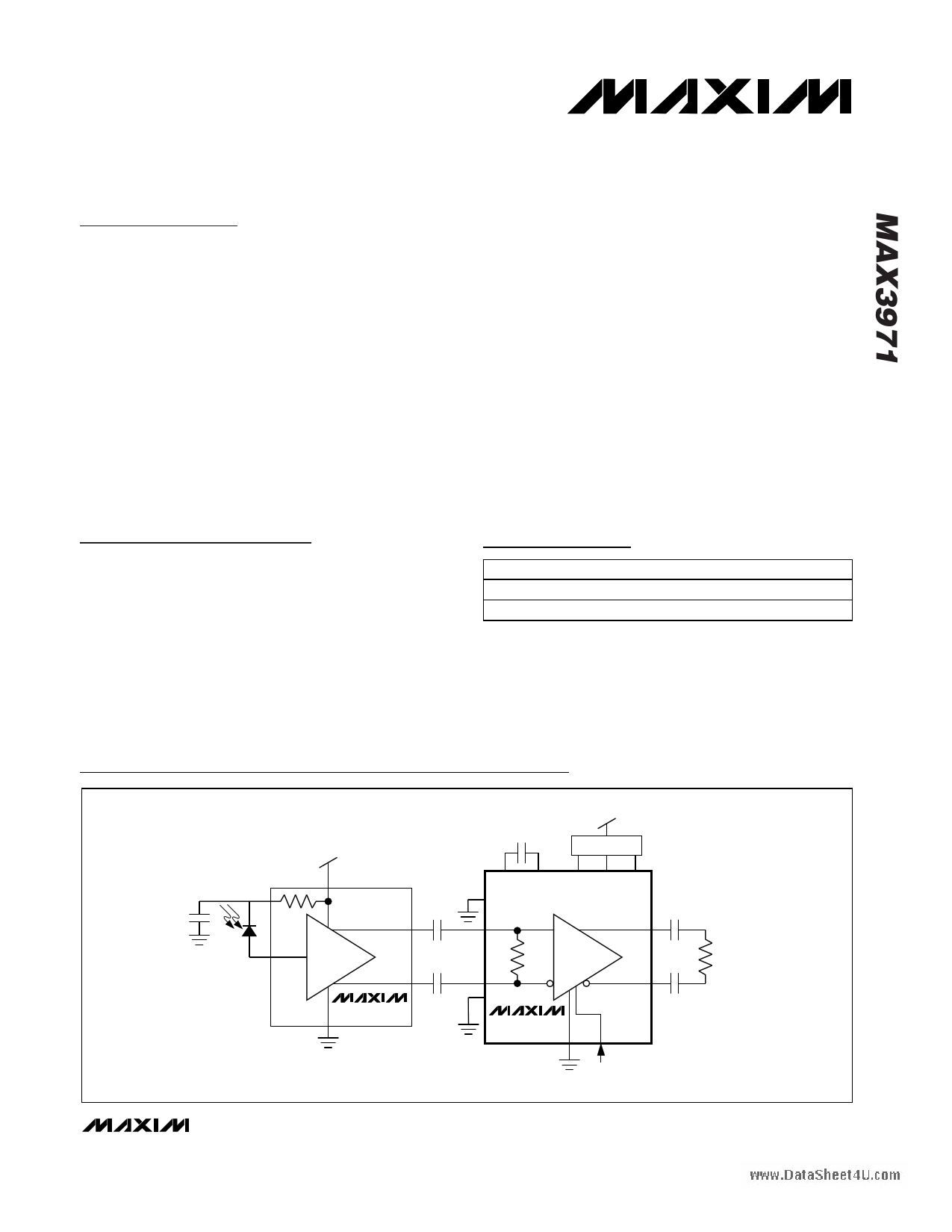
Typical Application Circuit
+3.3V
0.1µF
TIA
0.1µF
MAX3970
0.1µF
+3.3V
SUPPLY FILTER
CZ- CZ+
GNDIN+
IN+
VCC1 VCC2 VCC3
0.1µF
OUT+
100Ω
IN-
GNDIN-
MAX3971
0.1µF
OUT-
DISABLE
100Ω
________________________________________________________________ Maxim Integrated Products 1
For pricing, delivery, and ordering information, please contact Maxim/Dallas Direct! at
1-888-629-4642, or visit Maxim’s website at www.maxim-ic.com.
1 page 
+3.3V, 10.3Gbps Limiting Amplifier
Detailed Description and
Applications Information
Figure 1 is a functional diagram of the MAX3971 limit-
ing amplifier.The signal path consists of an input buffer
followed by a gain stage and output amplifier. A feed-
back loop provides offset correction by driving the
average value of the differential output to zero.
Gain Stage and Offset Correction
The limiting amplifier provides approximately 50dB
gain. This large gain makes the amplifier susceptible to
small DC offsets, which cause deterministic
jitter. A low-frequency loop is integrated into the limiting
amplifier to reduce output offset, typically to less than
2mV.
The external capacitor CZ is required to set the low-fre-
quency cutoff for the offset correction loop and for sta-
bility. The time constant of the loop is set by the
CZ
MAX3971
GNDIN+
IN+
INPUT
AMPLIFIER
IN-
GNDIN-
CZ- CZ+
OFFSET
CORRECTION
AMP
LOWPASS
FILTER
DISABLE
OUT+
GAIN OUTPUT
50dB AMPLIFIER
OUT-
product of an equivalent 20kΩ on-chip resistor and the
value of the off-chip capacitor, CZ. For stable opera-
tion, the minimum value of CZ is 0.01µF. To minimize
pattern-dependent jitter, CZ should be as large as pos-
sible. For 10-Gigabit Ethernet applications, the typical
value of CZ is 0.1µF. Keep CZ as close to the package
as possible.
CML Input Circuit
The input buffer is designed to accept CML input sig-
nals such as the output from the MAX3970 transimped-
ance amplifier. An equivalent circuit for the input is
shown in Figure 2. DC-coupling the inputs is not recom-
mended because doing so prevents the part’s offset
correction circuitry from working properly. Thus, AC-
coupling capacitors are required on the input.
CML Output Circuit
An equivalent circuit for the output network is shown in
Figure 3. It consists of two 50Ω resistors connected to
VCC driven by the collectors of an output differential
transistor pair (Q1 and Q2). The differential output sig-
nals are clamped by transistors Q3 and Q4 when the
DISABLE input is high.
Disable Function
A logic signal can be applied to the DISABLE pin to
squelch the output signal. When the output is disabled,
an offset is added to the output, preventing the follow-
ing stage from oscillating (if DC-coupled).
Figure 1. Functional Diagram
VCC1
GNDIN+
IN+
50Ω 50Ω
IN-
GNDIN-
ESD
STRUCTURES
DISABLE
Q3
DATA
Q4
VCC3
50Ω 50Ω
Q1 Q2
OUT+
OUT-
ESD
STRUCTURES
Figure 2. CML Input Equivalent Circuit
Figure 3. CML Input Equivalent Circuit Showing Clamping
Circuit for Squelching the Output Signal
_______________________________________________________________________________________ 5
5 Page | ||
| Páginas | Total 10 Páginas | |
| PDF Descargar | [ Datasheet MAX3971.PDF ] | |
Hoja de datos destacado
| Número de pieza | Descripción | Fabricantes |
| MAX397 | Precision / 16-Channel/Dual 8-Channel / Low-Voltage / CMOS Analog Multiplexers | Maxim Integrated |
| MAX3971 | 10.3Gbps Limiting Amplifier | Maxim Integrated Products |
| Número de pieza | Descripción | Fabricantes |
| SLA6805M | High Voltage 3 phase Motor Driver IC. |
Sanken |
| SDC1742 | 12- and 14-Bit Hybrid Synchro / Resolver-to-Digital Converters. |
Analog Devices |
|
DataSheet.es es una pagina web que funciona como un repositorio de manuales o hoja de datos de muchos de los productos más populares, |
| DataSheet.es | 2020 | Privacy Policy | Contacto | Buscar |