|
|
PDF IDT74SSTU32866B Data sheet ( Hoja de datos )
| Número de pieza | IDT74SSTU32866B | |
| Descripción | 1.8V CONFIGURABLE BUFFER | |
| Fabricantes | IDT | |
| Logotipo |  |
|
Hay una vista previa y un enlace de descarga de IDT74SSTU32866B (archivo pdf) en la parte inferior de esta página. Total 20 Páginas | ||
|
No Preview Available !
www.DataSheet4U.com
IDT74SSTUB32866B
1.8V CONFIGURABLE REGISTERED BUFFER WITH PARITY
1.8V CONFIGURABLE
BUFFER WITH PARITY
COMMERCIAL TEMPERATURE RANGE
IDT74SSTUB32866B
ADVANCE
INFORMATION
FEATURES:
• 1.8V Operation
• SSTL_18 style clock and data inputs
• Differential CLK input
• Configurable as 25-bit 1:1 or 14-bit 1:2 registered buffer
• Control inputs compatible with LVCMOS levels
• Flow-through architecture for optimum PCB design
• Latch-up performance exceeds 100mA
• ESD >2000V per MIL-STD-883, Method 3015; >200V using
machine model (C = 200pF, R = 0)
• Checks parity on data inputs
• Maximum operating frequency: 410MHz
• Optimized for DDR2 - 400 / 533 / 667 / 800 (PC2 - 3200 / 4300 /
5300 / 6400)
• JEDEC R/C E, F, G, H, and J
• Available in 96-pin LFBGA package
APPLICATIONS:
• Along with CSPUA877 DDR2 PLL, provides complete solution for
DDR2 DIMMs
DESCRIPTION:
This 25-bit 1:1 / 14-bit 1:2 configurable registered buffer is designed for
1.7V to 1.9V VDD operation. In the 1:1 pinout configuration, only one device
per DIMM is requred to drive nine SDRAM loads. In the 1:2 pinout
configuration, two devices per DIMM are required to drive eighteen
SDRAM loads. All inputs are SSTL_18, except reset (RESET) and control
(Cn) inputs, which are LVCMOS. All outputs are edge-controlled circuits
optimized for unterminated DIMM loads, and meet SSTL_18 specifications,
except the open-drain error (QERR) output.
The SSTUB32866B operates from a differential clock (CLK and CLK).
Data are registered at the crossing of CLK going high and CLK going low.
Parity is checked on the parity bit (PAR_IN) input which arrives one cycle
after the input data to which it applies. The QERR output is open drain.
When used as a single device, the C0 and C1 inputs are tied low. In this
configuration, the partial-parity-out (PPO) and QERR signals are produced
two clock cycles after the corresponding data output.
When used in pairs, the C0 input of the first register is tied low and the
C0 input of the second register is tied high. The C1 input of both registers
are tied high. The QERR output of the first SSTUB32866B is left floating and
the valid error information is latched on the QERR output of the second
SSTUB32866B.
If an error occurs and the QERR output is driven low, it stays latched low
for two clock cycles or until RESET is driven low. The DIMM-dependent
signals (DODT, DCKE, DCS, and CSR) are not included in the parity check.
The C0 input controls the pinout configuration of the 1:2 pinout from
register A configuration (when low) to register B configuration (when high).
The C1 input controls the pinout configurationfrom 25-bit 1:1 (when low) to
14-bit 1:2 (when high). C0 and C1 should not be switched during normal
operation. They should be hard-wired to a valid low or high level to
configure the register in the desired mode. In the 25-bit 1:1 pinout
configuration, the A6, D6, and H6 terminals are driven low and should not
be used.
The device supports low-power standby operation. When RESET is low,
the differential input recievers are disabled, and undriven (floating) data,
clock, and reference voltage (VREF) inputs are allowed. In addition, when
RESET is low, all registers are reset and all outputs except QERR are forced
low. The LVCMOS RESET and Cn inputs always must be held at a valid
logic high or low level.
There are two VREF pins (A3 and T3). However, it is necessary to only
connect one of the two VREF pins to the external VREF power supply. An
unused VREF pin should be terminated with a VREF coupling capacitor.
The device also supports low-power active operation by monitoring both
system chip select (DCS and CSR) inputs and will gate the Qn and PPO
outputs from changing states when both DCS and CSR inputs are high. If
either DCS or CSR input is low, the Qn and PPO outputs will function
normally. Also, if the internal low power signal (LPS1) is high, the device
will gate the QERR output from changing states. If LPS1 is low, the QERR
output will function normally. The RESET input has priority over the DCS
and CSR control and when driven low will force the Qn and PPO outputs
low, and the QERRoutput high. If the DCS control functionality is not desired,
then the CSR input can be hard-wired to ground, in which case the setup-
time requirement for DCS would be the same as for the other D data inputs.
To control the low-power mode with DCS only, then the CSR input should
be pulled up to VDD through a pullup resistor.
To ensure defined outputs from the register before a stable clock has been
supplied, RESET must be held in the low state during power up.
The IDT logo is a registered trademark of Integrated Device Technology, Inc.
COMMERCIAL TEMPERATURE RANGE
c 2005 Integrated Device Technology, Inc.
1
OCTOBER 2005
DSC 6892/3
1 page 
IDT74SSTUB32866B
1.8V CONFIGURABLE REGISTERED BUFFER WITH PARITY
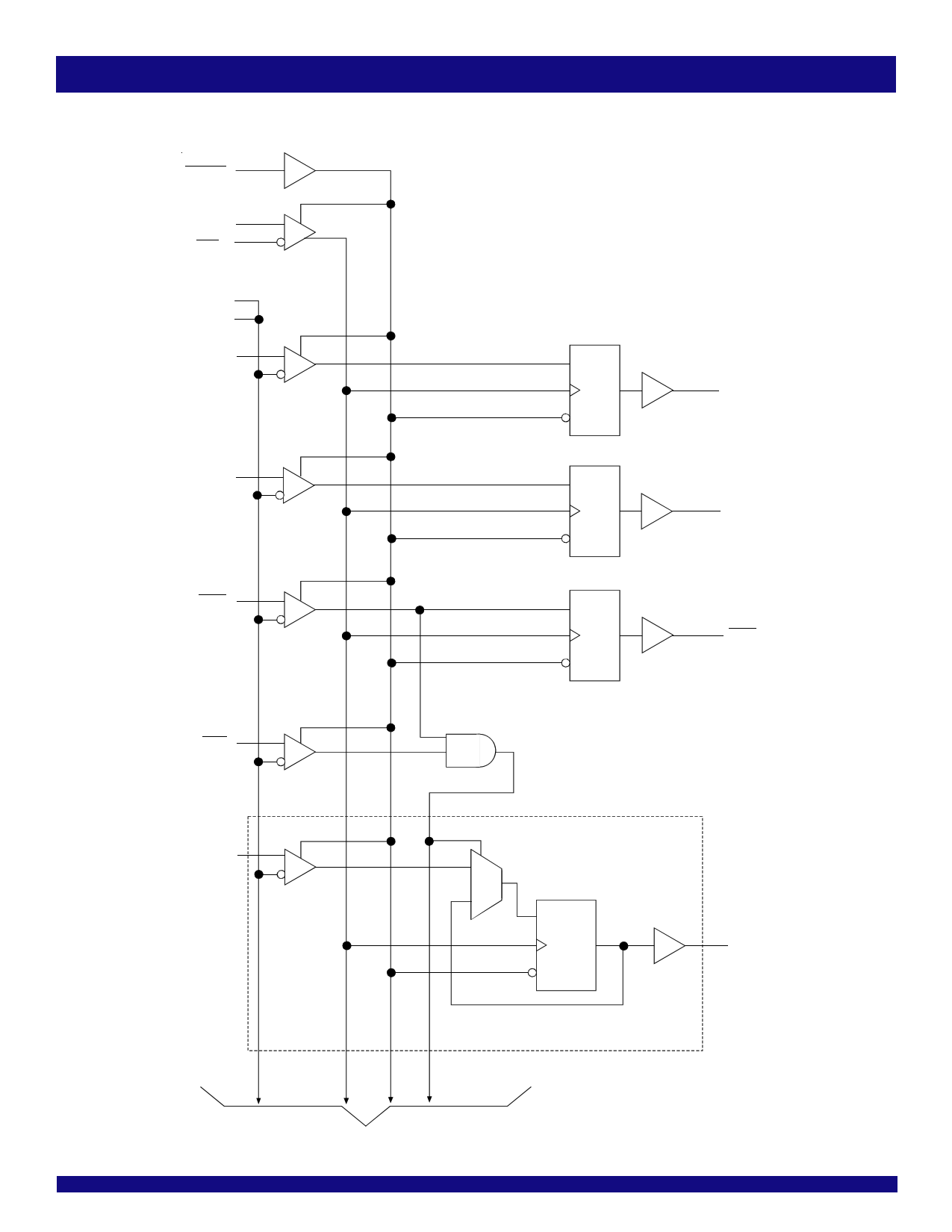
FUNCTIONAL BLOCK DIAGRAM (1:1)
RESET
CLK1
CLK1
VREF
DCKE
DODT
DCS
CSR
COMMERCIAL TEMPERATURE RANGE
1D
C1
R
1D
C1
R
1D
C1
R
QCKE
QOTD
QCS
D2
0
1
1D
C1
R
One of 22 Channels
TO 21 OTHER CHANNELS (D3, D5, D6, D8-D25)
5
Q2
5 Page 
IDT74SSTUB32866B
1.8V CONFIGURABLE REGISTERED BUFFER WITH PARITY
COMMERCIAL TEMPERATURE RANGE
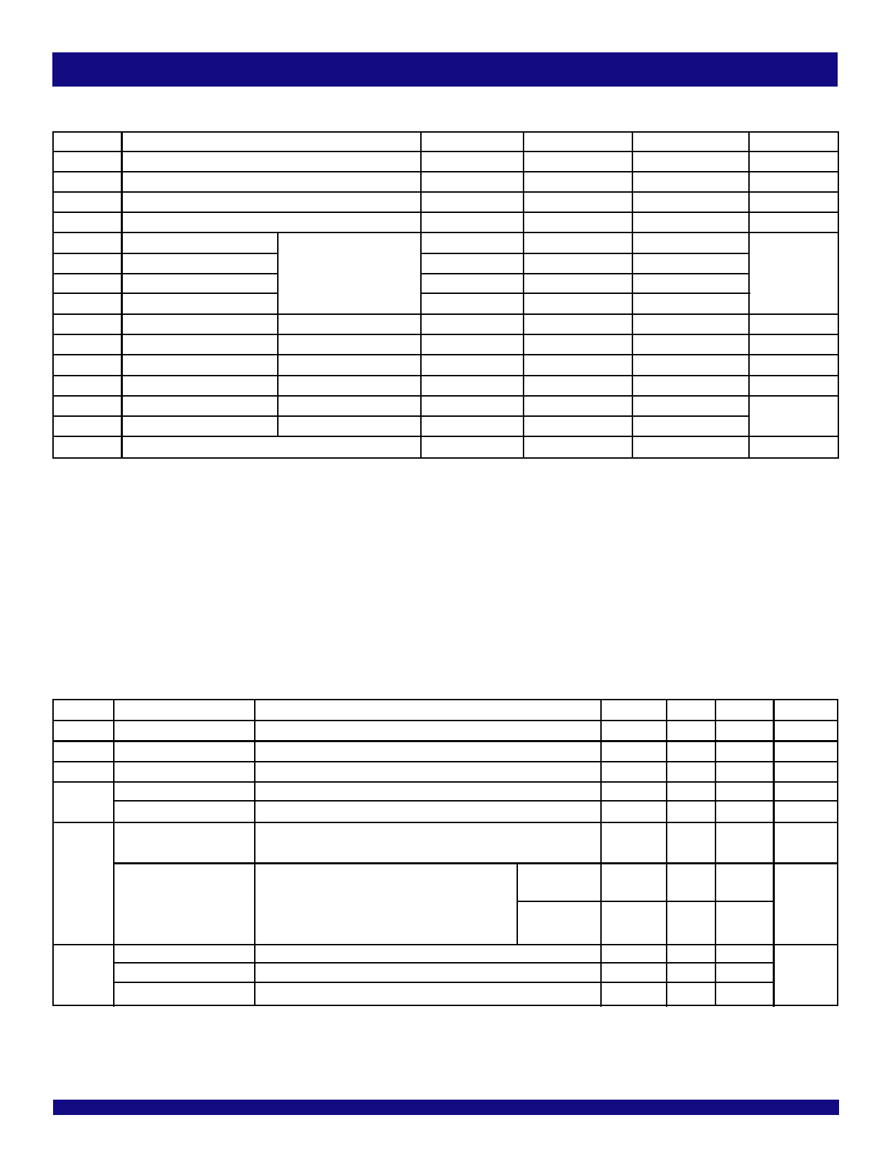
OPERATING CHARACTERISTICS, TA = 25ºC (1,2)
Symbol
Parameter
Min.
VDD Supply Voltage
1.7
VREF ReferenceVoltage
0.49 * VDD
VTT TerminationVoltage
VREF– 40mV
VI InputVoltage
0
VIH AC High-Level Input Voltage
VREF+ 250mV
VIL AC Low-Level Input Voltage Data Inputs, CSR, DCS,
—
VIH DC High-Level Input Voltage PAR_IN
VREF+ 125mV
VIL DC Low-Level Input Voltage
—
VIH
High-Level Input Voltage
RESET, Cx
0.65 * VDD
VIL
Low-Level Input Voltage
RESET, Cx
—
VICR Common Mode Input Voltage CLK, CLK
0.675
VID
Differential Input Voltage
CLK, CLK
600
IOH High-Level Output Current Data Outputs, PPO
—
IOL Low-Level Output Current Data Outputs, PPO, QERR
—
TA OperatingFree-AirTemperature
0
Typ.
—
0.5 * VDD
VREF
—
—
—
—
—
—
—
—
—
—
—
—
NOTES:
1. The RESET and Cx inputs of the device must be held at valid levels (not floating) to ensure proper device operation.
2. The differential inputs must not be floating unless RESET is LOW.
Max.
1.9
0.51 * VDD
VREF+ 40mV
VDD
—
VREF– 250mV
—
VREF– 125mV
—
0.35 * VDD
1.125
—
–8
8
70
Unit
V
V
V
V
V
V
V
V
mV
mA
°C
DC ELECTRICAL CHARACTERISTICS OVER OPERATING RANGE
Following Conditions Apply Unless Otherwise Specified:
Operating Condition: TA = 0°C to +70°C, VDD = 1.7V to 1.9V
Symbol Parameter
Test Conditions
VOH Output HIGH Voltage
IOH = –6 mA
VOL OutputLOWVoltage
IOL = 6 mA
II All Inputs(1)
VI = VDD or GND; VDD = 1.9V
IDD Static Standby
IO = 0, VDD = 1.9V, RESET = GND
Static Operating
IO = 0, VDD = 1.9V, RESET = VDD, VI = VIH (AC) or VIL (AC)
IDDD Dynamic Operating
IO = 0, VDD = 1.8V, RESET = VDD, VI = VIH (AC) or VIL (AC),
(Clock Only)
CLK and CLK Switching 50% Duty Cycle.
IO = 0, VDD = 1.8V, RESET = VDD,
1:1 Mode
Dynamic Operating
VI = VIH (AC) or VIL (AC), CLK and CLK Switching at
(Per Each Data Input)
50% Duty Cycle. One Data Input Switching at
1:2 Mode
Half Clock Frequency, 50% Duty Cycle.
Data Inputs, CSR, PAR_IN
CI CLK and CLK
VICR = 0.9V, VID = 600mV
RESET
VI = VDD or GND
NOTE:
1. Each VREF pin (A3, T3) should be tested independently, with the other pin open circuit.
Min. Typ.
1.2 —
——
——
——
——
——
——
——
2.5 —
2—
——
Max.
—
0.5
±5
100
40
—
—
—
3.5
3
—
Unit
V
V
μA
μA
mA
μA/Clock
MHz
μA/Clock
MHz/Data
Input
pF
11
11 Page | ||
| Páginas | Total 20 Páginas | |
| PDF Descargar | [ Datasheet IDT74SSTU32866B.PDF ] | |
Hoja de datos destacado
| Número de pieza | Descripción | Fabricantes |
| IDT74SSTU32866B | 1.8V CONFIGURABLE BUFFER | IDT |
| Número de pieza | Descripción | Fabricantes |
| SLA6805M | High Voltage 3 phase Motor Driver IC. |
Sanken |
| SDC1742 | 12- and 14-Bit Hybrid Synchro / Resolver-to-Digital Converters. |
Analog Devices |
|
DataSheet.es es una pagina web que funciona como un repositorio de manuales o hoja de datos de muchos de los productos más populares, |
| DataSheet.es | 2020 | Privacy Policy | Contacto | Buscar |
