|
|
|
PDF ICSSSTUB32872A Data sheet ( Hoja de datos )
| Número de pieza | ICSSSTUB32872A | |
| Descripción | 28-Bit Registered Buffer | |
| Fabricantes | ICS | |
| Logotipo | ||
Hay una vista previa y un enlace de descarga de ICSSSTUB32872A (archivo pdf) en la parte inferior de esta página. Total 18 Páginas | ||
|
No Preview Available !
www.DataSheet4U.com
Integrated
Circuit
Systems, Inc.
ICSSSTUB32872A
Advance Information
28-Bit Registered Buffer for DDR2
Recommended Application:
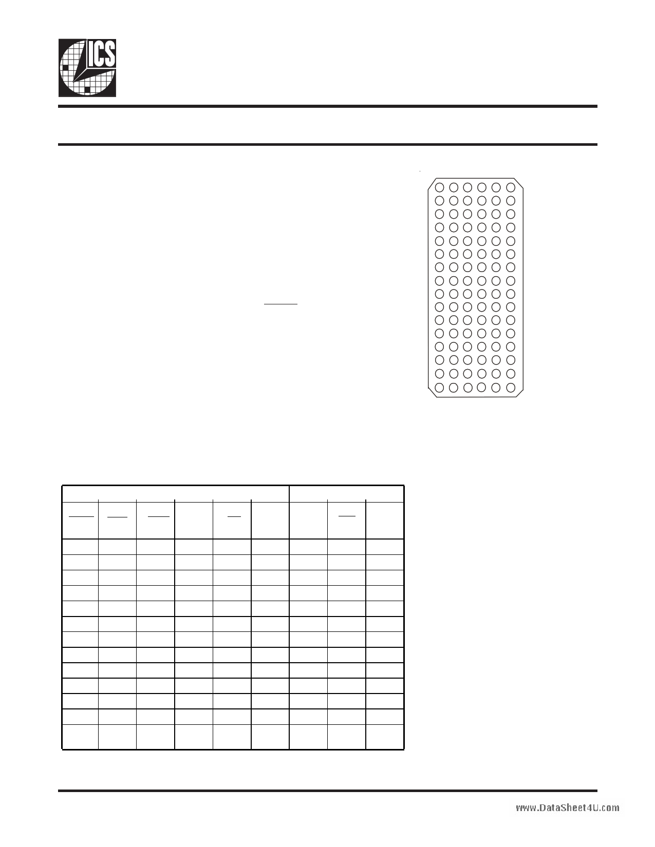
Pin Configuration
• DDR2 Memory Modules
123 45 6
• Provides complete DDR DIMM solution with
ICS98ULPA877A, ICS97ULP877, or IDTCSPUA877A
A
B
• Optimized for DDR2 400/533/667 JEDEC 4 Rank
VLP DIMMS
C
D
Product Features:
• 28-bit 1:1 registered buffer with parity check
functionality
• Supports SSTL_18 JEDEC specification on data
inputs and outputs
• Supports LVCMOS switching levels on RESET input
• 50% more dynamic driver strength than standard
SSTU32864
• Low voltage operation
VDD = 1.7V to 1.9V
• Available in 96 BGA package
E
F
G
H
J
K
L
M
N
P
R
T
96 Ball BGA
(Top View)
Functionality Truth Table
In puts
Outputs
RESET DCS0 DCS1 CK
Dn,
CK DODTn,
DCK En
Qn
QCS
QODT,
QCKE
H L L↑ ↓L L L L
HL
L↑
↓HH L
H
H
L
L L or H L or H
X
Q0 Q0 Q0
H L H↑ ↓ L L L L
H L H↑
↓HH L
H
H
L
H L or H L or H
X
Q0 Q0 Q0
H H L↑ ↓ L L H L
H H L↑
↓H H H H
H
H
L L or H L or H
X
Q0 Q0 Q0
H H H↑
↓ L Q0 H L
H H H↑
↓ H Q0 H H
H
H
H L or H L or H
X
Q0 Q0 Q0
L
X or X or
X or X or X or
floating floating floating floating floating
L
L
L
1222F—3/13/07
ADVANCE INFORMATION documents contain information on products in the formative or design phase development. Characteristic data and other specifications are design goals.
ICS reserves the right to change or discontinue these products without notice. Third party brands and names are the property of their respective owners.
1 page 
ICSSSTUB32872A
Advance Information
Block Diagram
VREF
PARIN
D0
D21
DCS0
DCS1
DCKE0,
DCKE1
DODT0,
DODT1
RESET
CK
CK
2
2
(CS ACTIVE)
DQ
R
PARITY
GENERATOR
22 AND
CHECKER
DQ
R
DQ
R
DQ
R
DQ
R
DQ
R
DQ
R
2
2
PTYERR
Q0
Q21
QCS0
QCS1
QCKE0,
QCKE1
QODT0,
QODT1
1222F—3/13/07
5
5 Page 
ICSSSTUB32872A
Advance Information
Electrical Characteristics - DC
TA = 0 - 70°C; VDD = 2.5 +/-0.2V, VDDQ=2.5 +/-0.2V; (unless otherwise stated)
SYMBOL PARAMETERS
CONDITIONS
VDDQ MIN TYP MAX UNITS
VOH IOH = -8mA
VOL IOL = 8mA
1.7V
1.7V
1.2
V
0.5
II All Inputs
VI = VDD or GND
Standby (Static) RESET = GND
1.9V
±5 µA
200 µA
IDD Operating (Static) VI = VIH(AC) or VIL(AC),
RESET = VDD
1.9V
mA
150
Dynamic operating
(clock only)
RESET = VDD,
VI = VIH(AC) or VIL(AC),
CLK and CLK switching
TBD
µA/clock
MHz
50% duty cycle.
RESET = VDD,
IO = 0
IDDD
VI = VIH(AC) or VIL (AC),
Dynamic Operating CLK and CLK switching
(per each data
50% duty cycle. One data
input)
input switching at half
1.8V
TBD
µA/ clock
MHz/data
clock frequency, 50%
duty cycle
Data Inputs
Ci CLK and CLK
RESET
VI = VREF ±350mV
VICR = 1.25V, VI(PP) = 360mV
VI = VDDQ or GND
2.5 5
2 3.8
4.5
pF
pF
Notes:
1 - Guaranteed by design, not 100% tested in production.
Output Buffer Characteristics
Output edge rates over recommended operating free-air temperature range (See figure 7)
PARAMETER
VDD = 1.8V ± 0.1V
MIN MAX
UNIT
dV/dt_r
1
4
V/ns
dV/dt_f
dV/dt_Δ1
1
4
1
V/ns
V/ns
1. Difference between dV/dt_r (rising edge rate) and dV/dt_f (falling edge rate)
1222F—3/13/07
11
11 Page | ||
| Páginas | Total 18 Páginas | |
| PDF Descargar | [ Datasheet ICSSSTUB32872A.PDF ] | |
Hoja de datos destacado
| Número de pieza | Descripción | Fabricantes |
| ICSSSTUB32872A | 28-Bit Registered Buffer | ICS |
| Número de pieza | Descripción | Fabricantes |
| SLA6805M | High Voltage 3 phase Motor Driver IC. |
Sanken |
| SDC1742 | 12- and 14-Bit Hybrid Synchro / Resolver-to-Digital Converters. |
Analog Devices |
|
DataSheet.es es una pagina web que funciona como un repositorio de manuales o hoja de datos de muchos de los productos más populares, |
| DataSheet.es | 2020 | Privacy Policy | Contacto | Buscar |