|
|
|
PDF 89HPES48H12 Data sheet ( Hoja de datos )
| Número de pieza | 89HPES48H12 | |
| Descripción | 48-Lane 12-Port PCI Express System Interconnect Switch | |
| Fabricantes | IDT | |
| Logotipo | ||
Hay una vista previa y un enlace de descarga de 89HPES48H12 (archivo pdf) en la parte inferior de esta página. Total 30 Páginas | ||
|
No Preview Available !
www.DataSheet4U.com
48-Lane 12-Port PCI Express®
System Interconnect Switch
®
89HPES48H12
Data Sheet
Device Overview
The 89HPES48H12 is a member of the IDT PRECISE™ family of
PCI Express® switching solutions. The PES48H12 is a 48-lane, 12-port
system interconnect switch optimized for PCI Express packet switching
in high-performance applications, supporting multiple simultaneous
peer-to-peer traffic flows. Target applications include servers, storage,
communications, and embedded systems.
Features
◆ High Performance PCI Express Switch
– Twelve maximum switch ports
• Six main ports each of which consists of 8 SerDes
• Each x8 main port can further bifurcate to 2 x4-ports
– Forty-eight 2.5 Gbps embedded SerDes
• Supports pre-emphasis and receive equalization on per-port
basis
– Delivers 192 Gbps (24 GBps) of aggregate switching capacity
– Low-latency cut-through switch architecture
– Support for Max Payload Size up to 2048 bytes
– Supports two virtual channels and eight traffic classes
– PCI Express Base Specification Revision 1.1 compliant
◆ Flexible Architecture with Numerous Configuration Options
– Port arbitration schemes utilizing round robin algorithms
– Virtual channels arbitration based on priority
– Automatic per port link width negotiation to x8, x4, x2 or x1
– Supports automatic lane reversal on all ports
– Supports automatic polarity inversion on all lanes
– Supports locked transactions, allowing use with legacy soft-
ware
– Ability to load device configuration from serial EEPROM
– Ability to control device via SMBus
◆ Highly Integrated Solution
– Requires no external components
– Incorporates on-chip internal memory for packet buffering and
queueing
– Integrates forty-eight 2.5 Gbps embedded full duplex SerDes,
8B/10B encoder/decoder (no separate transceivers needed)
◆ Reliability, Availability, and Serviceability (RAS) Features
– Redundant upstream port failover capability
– Supports optional PCI Express end-to-end CRC checking
– Internal end-to-end parity protection on all TLPs ensures data
integrity even in systems that do not implement end-to-end
CRC (ECRC)
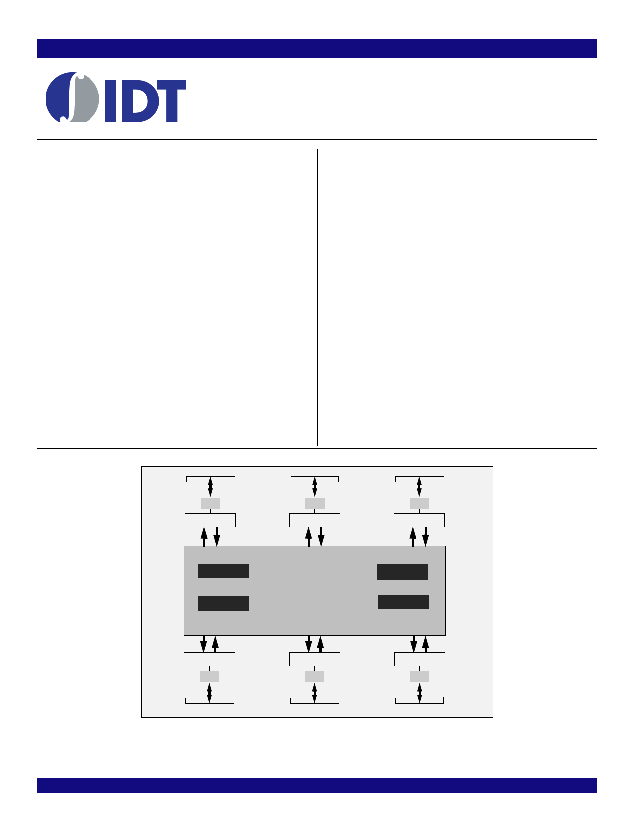
Block Diagram
x8/x4/x2/x1
x8/x4/x2/x1
x8/x4/x2/x1
SerDes
DL/Transaction Layer
SerDes
DL/Transaction Layer
SerDes
DL/Transaction Layer
Route Table
Frame Buffer
12-Port Switch Core
Port
Arbitration
Scheduler
DL/Transaction Layer
SerDes
DL/Transaction Layer
SerDes
DL/Transaction Layer
SerDes
x8/x4/x2/x1
x8/x4/x2/x1
x8/x4/x2/x1
© 2007 Integrated Device Technology, Inc.
48 PCI Express Lanes
Up to 6 x8 ports or 12 x4 Ports
Figure 1 Internal Block Diagram
IDT and the IDT logo are registered trademarks of Integrated Device Technology, Inc.
1 of 48
July 19, 2007
DSC 6925
1 page 
IDT 89HPES48H12 Data Sheet
Signal
PE7TP[3:0]
PE7TN[3:0]
PE8RP[3:0]
PE8RN[3:0]
PE8TP[3:0]
PE8TN[3:0]
PE9RP[3:0]
PE9RN[3:0]
PE9TP[3:0]
PE9TN[3:0]
PE10RP[3:0]
PE10RN[3:0]
PE10TP[3:0]
PE10TN[3:0]
PE11RP[3:0]
PE11RN[3:0]
PE11TP[3:0]
PE11TN[3:0]
REFCLKM
REFCLKP[3:0]
REFCLKN[3:0]
Type
Name/Description
O PCI Express Port 7 Serial Data Transmit. Differential PCI Express transmit pairs for
port 7. When port 6 is merged with port 7, these signals become port 6 transmit pairs
for lanes 4 through 7.
I PCI Express Port 8 Serial Data Receive. Differential PCI Express receive pairs for
port 8.
O PCI Express Port 8 Serial Data Transmit. Differential PCI Express transmit pairs for
port 8.
I PCI Express Port 9 Serial Data Receive. Differential PCI Express receive pairs for
port 9. When port 8 is merged with port 9, these signals become port 8 receive pairs
for lanes 4 through 7.
O PCI Express Port 9 Serial Data Transmit. Differential PCI Express transmit pairs for
port 9. When port 8 is merged with port 9, these signals become port 8 transmit pairs
for lanes 4 through 7.
I PCI Express Port 10 Serial Data Receive. Differential PCI Express receive pairs for
port 10.
O PCI Express Port 10 Serial Data Transmit. Differential PCI Express transmit pairs
for port 10.
I PCI Express Port 11 Serial Data Receive. Differential PCI Express receive pairs for
port 11. When port 10 is merged with port 11, these signals become port 10 receive
pairs for lanes 4 through 7.
O PCI Express Port 11 Serial Data Transmit. Differential PCI Express transmit pairs
for port 11. When port 10 is merged with port 11, these signals become port 10 trans-
mit pairs for lanes 4 through 7.
I PCI Express Reference Clock Mode Select. This signal selects the frequency of the
reference clock input.
0x0 - 100 MHz
0x1 - 125 MHz
I PCI Express Reference Clock. Differential reference clock pair input. This clock is
used as the reference clock by on-chip PLLs to generate the clocks required for the
system logic and on-chip SerDes. The frequency of the differential reference clock is
determined by the REFCLKM signal.
Table 2 PCI Express Interface Pins (Part 2 of 2)
Signal
MSMBADDR[4:1]
MSMBCLK
MSMBDAT
Type
Name/Description
I Master SMBus Address. These pins determine the SMBus address of the serial
EEPROM from which configuration information is loaded.
I/O Master SMBus Clock. This bidirectional signal is used to synchronize transfers on the
master SMBus. It is active and generating the clock only when the EEPROM or I/O
Expanders are being accessed.
I/O Master SMBus Data. This bidirectional signal is used for data on the master SMBus.
Table 3 SMBus Interface Pins (Part 1 of 2)
5 of 48
July 19, 2007
5 Page 
IDT 89HPES48H12 Data Sheet
Pin Characteristics
Note: Some input pads of the PES48H12 do not contain internal pull-ups or pull-downs. Unused inputs should be tied off to appropriate
levels. This is especially critical for unused control signal inputs which, if left floating, could adversely affect operation. Also, any input pin left
floating can cause a slight increase in power consumption.
Function
PCI Express Interface
Pin Name
PE0RN[3:0]
PE0RP[3:0]
PE0TN[3:0]
PE0TP[3:0]
PE1RN[3:0]
PE1RP[3:0]
PE1TN[3:0]
PE1TP[3:0]
PE2RN[3:0]
PE2RP[3:0]
PE2TN[3:0]
PE2TP[3:0]
PE3RN[3:0]
PE3RP[3:0]
PE3TN[3:0]
PE3TP[3:0]
PE4RN[3:0]
PE4RP[3:0]
PE4TN[3:0]
PE4TP[3:0]
PE5RN[3:0]
PE5RP[3:0]
PE5TN[3:0]
PE5TP[3:0]
PE6RN[3:0]
PE6RP[3:0]
PE6TN[3:0]
PE6TP[3:0]
PE7RN[3:0]
PE7RP[3:0]
PE7TN[3:0]
PE7TP[3:0]
Type
I
I
O
O
I
I
O
O
I
I
O
O
I
I
O
O
I
I
O
O
I
I
O
O
I
I
O
O
I
I
O
O
Buffer
CML
I/O Internal
Type Resistor
Serial Link
Table 8 Pin Characteristics (Part 1 of 3)
Notes
11 of 48
July 19, 2007
11 Page | ||
| Páginas | Total 30 Páginas | |
| PDF Descargar | [ Datasheet 89HPES48H12.PDF ] | |
Hoja de datos destacado
| Número de pieza | Descripción | Fabricantes |
| 89HPES48H12 | 48-Lane 12-Port PCI Express System Interconnect Switch | IDT |
| Número de pieza | Descripción | Fabricantes |
| SLA6805M | High Voltage 3 phase Motor Driver IC. |
Sanken |
| SDC1742 | 12- and 14-Bit Hybrid Synchro / Resolver-to-Digital Converters. |
Analog Devices |
|
DataSheet.es es una pagina web que funciona como un repositorio de manuales o hoja de datos de muchos de los productos más populares, |
| DataSheet.es | 2020 | Privacy Policy | Contacto | Buscar |