|
|
|
PDF RF5111 Data sheet ( Hoja de datos )
| Número de pieza | RF5111 | |
| Descripción | 3V DCS POWER AMPLIFIER | |
| Fabricantes | RF Micro Devices | |
| Logotipo | ||
Hay una vista previa y un enlace de descarga de RF5111 (archivo pdf) en la parte inferior de esta página. Total 14 Páginas | ||
|
No Preview Available !
www.DataSheet4U.com
RF5111
0 3V DCS POWER AMPLIFIER
RoHS Compliant & Pb-Free Product
Typical Applications
• 3V DCS1800 (PCN) Cellular Handsets
• Commercial and Consumer Systems
• 3V DCS1900 (PCS) Cellular Handsets
• 3V Dual-Band/Triple-Band Handsets
• Portable Battery-Powered Equipment
• GPRS Compatible
Product Description
The RF5111 is a high-power, high-efficiency power ampli-
fier module offering high performance in GSM or GPRS
applications. The device is manufactured on an advanced
GaAs HBT process, and has been designed for use as
the final RF amplifier in DCS1800/1900 handheld digital
cellular equipment and other applications in the
1700MHz to 2000MHz band. On-board power control
provides over 65dB of control range with an analog volt-
age input, and provides power down with a logic “low” for
standby operation. The device is self-contained with 50Ω
input and the output can be easily matched to obtain opti-
mum power and efficiency characteristics. The RF5111
can be used together with the RF5110 for dual-band
operation. The device is packaged in an ultra-small plas-
tic package, minimizing the required board space.
Optimum Technology Matching® Applied
Si BJT
9GaAs HBT
GaAs MESFET
Si Bi-CMOS
SiGe HBT
Si CMOS
InGaP/HBT
GaN HEMT
SiGe Bi-CMOS
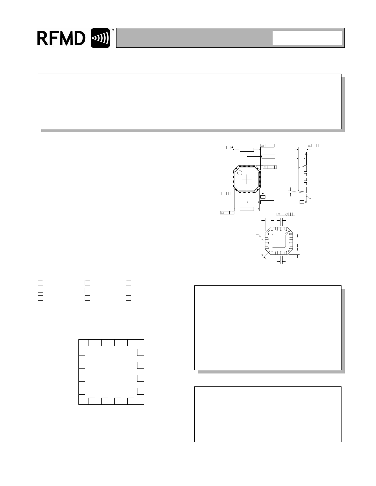
16 15 14 13
VAT EN 1
12 RF OUT
RF IN 2
11 RF OUT
GND1 3
10 RF OUT
VCC1 4
9 NC
5678
-A-
3.00 SQ.
0.15 C A
2 PLCS
1.50 TYP
2 PLCS
0.15 C B
1.00
0.85
0.80
0.65
0.05 C
0.05
0.01
2 PLCS
0.15 C B
-B-
1.37 TYP
12°
MAX
2 PLCS
0.15 C A
2.75 SQ.
Shaded lead is pin 1.
0.60
0.24
TYP
Dimensions in mm.
0.10 M C A B
0.30
0.18
-C-
0.45
0.00
4 PLCS
11..6355SQ.
0.23
0.13
4 PLCS
0.50
0.55
0.30
SEATING
PLANE
Package Style: QFN, 16-Pin, 3x3
Features
• Single 2.7V to 4.8V Supply Voltage
• +33dBm Output Power at 3.5V
• 27dB Gain with Analog Gain Control
• 50% Efficiency
• 1700MHz to 1950MHz Operation
• Supports DCS1800 and PCS1900
Ordering Information
RF5111
3V DCS Power Amplifier
RF5111PCBA-41X Fully Assembled Evaluation Board
Functional Block Diagram
RF Micro Devices, Inc.
7628 Thorndike Road
Greensboro, NC 27409, USA
Tel (336) 664 1233
Fax (336) 664 0454
http://www.rfmd.com
Rev A1 060921
2-1
1 page 
RF5111
Pin Function Description
Interface Schematic
14
VCC2
Power supply for the driver stage. This pin forms the shunt inductance
needed for proper tuning of the second interstage match.
VCC2
15
16
Pkg
Base
VCC2
VCC2
GND
From Bias
Stages GND2
Same as pin 14.
Same as pin 14.
Same as pin 14.
Same as pin 14.
Ground connection for the output stage. This pad should be connected
to the groundplane by vias directly under the device. A short path is
required to obtain optimum performance, as well as to provide a good
thermal path to the PCB for maximum heat dissipation.
Rev A1 060921
2-5
5 Page 
RF5111
Evaluation Board Layout
Board Size 2.0” x 2.0”
Board Thickness 0.032”, Board Material FR-4, Multi-Layer
Rev A1 060921
2-11
11 Page | ||
| Páginas | Total 14 Páginas | |
| PDF Descargar | [ Datasheet RF5111.PDF ] | |
Hoja de datos destacado
| Número de pieza | Descripción | Fabricantes |
| RF5110 | 3V GSM POWER AMPLIFIER | RF Micro Devices |
| RF5110G | 3V GSM POWER AMPLIFIER | RF Micro Devices |
| RF5111 | 3V DCS POWER AMPLIFIER | RF Micro Devices |
| RF5112 | 2.4GHz TO 2.5GHz LINEAR POWER AMPLIFIER | RF Micro Devices |
| Número de pieza | Descripción | Fabricantes |
| SLA6805M | High Voltage 3 phase Motor Driver IC. |
Sanken |
| SDC1742 | 12- and 14-Bit Hybrid Synchro / Resolver-to-Digital Converters. |
Analog Devices |
|
DataSheet.es es una pagina web que funciona como un repositorio de manuales o hoja de datos de muchos de los productos más populares, |
| DataSheet.es | 2020 | Privacy Policy | Contacto | Buscar |