|
|
|
PDF RF3159 Data sheet ( Hoja de datos )
| Número de pieza | RF3159 | |
| Descripción | QUAD-BAND GSM/EDGE/GSM850/EGSM900 /DCS/PCS/POWER AMPLIFIER MODULE | |
| Fabricantes | RF Micro Devices | |
| Logotipo | ||
Hay una vista previa y un enlace de descarga de RF3159 (archivo pdf) en la parte inferior de esta página. Total 26 Páginas | ||
|
No Preview Available !
www.DataSheet4U.com
RF3159
QUAD-BAND GSM/EDGE/GSM850/EGSM900
/DCS/PCS/POWER AMPLIFIER MODULE
RoHS Compliant & Pb-Free Product
Package Style: Module (6mmx6mm)
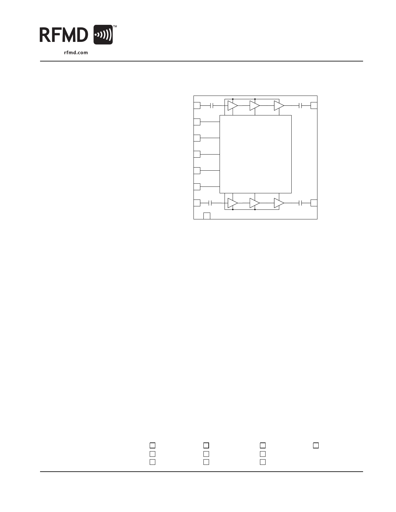
HB RFIN 1
18 HB RFOUT
Features
High Gain for use in Systems
with Low RF Driver Power
Linear EDGE and GSM Opera-
tion
PowerStar® GSM/GPRS
Power Control
Digital Band Select Enables
GSM850, EGSM900 or DCS,
PCS Amplifier Lineup
Single Supply Voltage;
Requires no External Refer-
ence Voltage
Automatic VBATT Tracking Cir-
cuit avoids Switching Tran-
sients at Low Supply Voltage
Low Power Mode for Reduced
EDGE Current
Digital Bias Control for Simple
Implementation of Low Power
Mode
Compact 6mmx6mm Pack-
age
Applications
Quad-Band GSM/EDGE
Handsets
GSM/EDGE Transmitter Line-
ups
Portable Battery-Powered
Equipment
GSM850/EGSM900/DCS/
PCS Products
GPRS Class 12 Compatible
Products
Mobile EDGE/GPRS Data
Products
BAND SEL 2
TX EN 3
VBATT 4
VMODE 5
VRAMP 6
LB RFIN 7
8
Integrated Power
Control
12 LB RFOUT
Functional Block Diagram
Product Description
The RF3159 is a high power, dual-mode amplifier module with integrated
power control. The input and output terminals are internally matched to
50Ω. The amplifier devices are manufactured on an advanced Gallium
Arsenide Heterojunction Bipolar Transistor (GaAs HBT) process, which is
designed to operate either in saturated mode for GMSK signaling or linear
mode for 8PSK signaling. The module is designed to be the final amplifica-
tion stage in a dual-mode GSM/EDGE mobile transmit lineup operating in
the 824MHz to 915MHz (low) and 1710MHz to 1910MHz (high) bands
(such as a cellular handset). Band selection is controlled by an input on
the module which selects either the low or high band. The device is pack-
aged on a 6mmx6mm laminate module with a protective plastic over-
mold.
Ordering Information
RF3159 Quad-Band GSM/EDGE/GSM850/EGSM900RF3159Quad-Band GSM/EDGE/GSM850/EGSM900 /DCS/PCS/Power Amplifier Module
/DCS/PCS/Power Amplifier Module
Power Amplifier Module, 5 Piece Sample Pack
RF3159PCBA-41X Fully Assembled Evaluation Board
Optimum Technology Matching® Applied
9GaAs HBT
GaAs MESFET
SiGe BiCMOS
Si BiCMOS
9GaAs pHEMT
Si CMOS
GaN HEMT
InGaP HBT
SiGe HBT
Si BJT
RF MICRO DEVICES®, RFMD®, Optimum Technology Matching®, Enabling Wireless Connectivity™, PowerStar®, POLARIS™ TOTAL RADIO™ and UltimateBlue™ are trademarks of RFMD, LLC. BLUETOOTH is a trade-
mark owned by Bluetooth SIG, Inc., U.S.A. and licensed for use by RFMD. All other trade names, trademarks and registered trademarks are the property of their respective owners. ©2006, RF Micro Devices, Inc.
Rev A0 DS070102
7628 Thorndike Road, Greensboro, NC 27409-9421 · For sales or technical
support, contact RFMD at (+1) 336-678-5570 or [email protected].
1 of 26
1 page 
RF3159
Parameter
Specification
Min. Typ. Max.
EGSM 900MHz Band
GMSK Mode
Operating Frequency Range
Input Power Range, PIN
Maximum Output Power 1
Maximum Output Power 2
Total Efficiency (PAE)
Output Noise Power
880
-2
34.2
32.0
47
+1
34.8
33.5
55
-81
915
+4
-78
-85 -82
Forward Isolation 1
Forward Isolation 2
2f0 Harmonics
3f0 Harmonics
Fundamental Cross Band Coupling
2f0, 3f0 Cross Band Coupling
All Other Non-harmonic Spurious
Input VSWR
Output Load VSWR Stability
-32
-10
-15 -5
-30 -10
-10
-20
-36
3:1
5:1
Output Load VSWR Ruggedness
10:1
Note: VRAMP,MAX=2.2V, VRAMP,MIN=0.30V, Rated POUT=34.2dBm
Unit
MHz
dBm
dBm
dBm
%
dBm
dBm
dBm
dBm
dBm
dBm
dBm
dBm
dBm
Condition
Nominal Conditions (unless otherwise stated):
Input and Output=50Ω, Temp=25 °C,
VCC=3.6V, VMODE=”Low”, Freq=880MHz to
915MHz, 25% Duty Cycle, Pulse
Width=1154μs, PIN=-2dBm,
BAND_SEL=“Low”, TX_EN=“High”,
VRAMP= VRAMP,MAX
Temp=25°C, VCC=3.6V
Temp=+85oC, VCC=3.2V
RBW=100kHz, 925MHz to 935MHz,
f0=915MHz, Over PIN range,
POUT<Rated POUT
RBW=100kHz, 935MHz to 960MHz,
f0=915MHz, over PIN range,
POUT<Rated POUT
TX_EN=0V, VRAMP=VRAMP,MIN,
PIN = +4 dBm
VRAMP=VRAMP,MIN, PIN=+4dBm
Measured at HB_RFOUT pin,
POUT<Rated POUT at LB_RFOUT pin.
Measured at HB_RFOUT pin,
POUT<Rated POUT at LB_RFOUT pin.
Over PIN range, POUT<Rated POUT
Spurious<-36dBm, Set VRAMP where
POUT<Rated POUT into 50Ω load, Full PIN
Range, RBW=3MHz
Set VRAMP where POUT<Rated POUT into 50Ω
load, no damage or permanent degradation to
part
Rev A0 DS070102
7628 Thorndike Road, Greensboro, NC 27409-9421 · For sales or technical
support, contact RFMD at (+1) 336-678-5570 or [email protected].
5 of 26
5 Page 
RF3159
Pin Function Description
1
HB_RFIN
RF input to the high-band PA. It is DC-blocked within the part.
2 BAND_SEL Digital input enables either the low band or high band amplifier die within the module. A logic low selects Low
Band (GSM850/EGSM900), a low logic high selects High Band (DCS1800/PCS1900). This pin is a high imped-
ance CMOS input with no pull-up or pull-down resistors.
3
TX_EN
Digital input enables or disables the internal circuitry. When disabled, the module is in the OFF state, and
draws virtually zero current. This pin is a high impedance CMOS input with no pull-up or pull-down resistors.
4
VBATT
Main DC power supply for all circuitry in the RF3159. Traces to this pin will have high current pulses during
operation so proper decoupling and routing should be observed.
5
VMODE
Digital input which internally adjusts settings to optimize amplifier performance for saturated or linear mode. A
logic low selects saturated mode for GMSK modulation. A logic high selects linear mode for 8PSK modulation.
This pin is a high impedance CMOS input with no pull-up or pull-down resistors.
6
VRAMP
In GMSK mode, the voltage on this pin controls the output power by varying the regulated collector voltage of
the amplifiers. In EDGE mode, this pin has no effect. An internal 300kHz filter reduces switching ORFS result-
ing from transitions between DAC steps. Most systems will have no need for external VRAMP filtering. This pin
provides an impedance of approximately 60kΩ.
7
LB_RFIN
RF input to the low-band PA. It is DC-blocked within the part.
8
VBIAS
Bias selection logic pin. A logic low selects a low bias (current saving mode) which will only meet linearity per-
formance at low power levels. A logic high allows linear performance up to the highest supported output power.
9
GND
Ground.
10
GND
Ground.
11
GND
Ground.
12 LB_RFOUT RF output from the low-band PA. It is DC-blocked within the part.
13
GND
Ground.
14
GND
Ground.
15
GND
Ground.
16
GND
Ground.
17
GND
Ground.
18 HB_RFOUT RF output from the high-band PA. It is DC-blocked within the part.
19
GND
Ground.
20
GND
Ground.
21
GND
Ground.
22
GND
Ground.
23
GND
Main ground pad in center of part. This pad should be tied to the main ground plane with as little loss as pos-
sible for optimum linearity.
Rev A0 DS070102
7628 Thorndike Road, Greensboro, NC 27409-9421 · For sales or technical
support, contact RFMD at (+1) 336-678-5570 or [email protected].
11 of 26
11 Page | ||
| Páginas | Total 26 Páginas | |
| PDF Descargar | [ Datasheet RF3159.PDF ] | |
Hoja de datos destacado
| Número de pieza | Descripción | Fabricantes |
| RF3158 | QUAD-BAND GSM/EDGE/GSM850/EGSM900 /DCS/PCS POWER AMPLIFIER MODULE | RF Micro Devices |
| RF3159 | QUAD-BAND GSM/EDGE/GSM850/EGSM900 /DCS/PCS/POWER AMPLIFIER MODULE | RF Micro Devices |
| Número de pieza | Descripción | Fabricantes |
| SLA6805M | High Voltage 3 phase Motor Driver IC. |
Sanken |
| SDC1742 | 12- and 14-Bit Hybrid Synchro / Resolver-to-Digital Converters. |
Analog Devices |
|
DataSheet.es es una pagina web que funciona como un repositorio de manuales o hoja de datos de muchos de los productos más populares, |
| DataSheet.es | 2020 | Privacy Policy | Contacto | Buscar |