|
|
PDF XRD8799 Data sheet ( Hoja de datos )
| Número de pieza | XRD8799 | |
| Descripción | A/D CONVERTER | |
| Fabricantes | Exar Corporation | |
| Logotipo |  |
|
Hay una vista previa y un enlace de descarga de XRD8799 (archivo pdf) en la parte inferior de esta página. Total 23 Páginas | ||
|
No Preview Available !
xrwww.DataSheet4U.com
XRD8799
FEBRUARY 2001
LOW POWER, 2 MSPS, 10-BIT, A/D CONVERTER WITH 8-CHANNEL MUX
REV. 1.00
FEATURES
• 10-Bit Resolution
• 8-Channel Mux
• Sampling Rate - < 1kHz - 2MHz
• Low Power CMOS - 35 mW (typ)
• Power Down; Lower Consumption - 0.8 mW (typ)
• Input Range between GND and VDD
• No S/H Required for Analog Signals less than
100kHz
• No S/H Required for CCD Signals less than 2MHz
• Single Power Supply (4.5 to 5.5V)
• Latch-Up Free
• ESD Protection: 2000 Volts Minimum
APPLICATIONS
• µP/DSP Interface and Control Application
• High Resolution Imaging - Scanners & Copiers
• Wireless Digital Communications
• Multiplexed Data Acquisition
BENEFITS
• Reduced Board Space (Small Package)
• Reduced External Parts, No Sample/Hold Needed
• Suitable for Battery & Power Critical Applications
• Designer can Adapt Input Range & Scaling
GENERAL DESCRIPTION
The XRD8799 is a flexible, easy to use, precision 10-
bit analog-to-digital converter with 8-channel mux that
operates over a wide range of input and sampling
conditions. The XRD8799 can operate with pulsed
"on demand" conversion operation or continuous
"pipeline" operation for sampling rates up to 2MHz.
The elimination of the S/H requirements, very low
power, and small package size offer the designer a
low cost solution. No sample and hold is required for
CCD applications up to 2MHz, or multiplexed input
applications when the signal source bandwidth is lim-
ited to 100kHz. The input architecture of the
XRD8799 allows direct interface to any analog input
range between AGND and AVDD (0 to 1V, 1 to 4V, 0 to
5V, etc.). The user simply sets VREF(+) and VREF(-) to
encompass the desired input range.
Scaled reference resistor taps @ 1/4 R, 1/2 R and 3/4
R allow for customizing the transfer curve as well as
providing a 1/2 span reference voltage. Digital out-
puts are CMOS and TTL compatible.
The XRD8799 uses a two-step flash technique. The
first segment converts the 5 MSBs and consists of
autobalanced comparators, latches, an encoder, and
buffer storage registers. The second segment con-
verts the remaining 5 LSBs.
When the power down input is "high", the data out-
puts DB9 to DB0 hold the current values and VREF(-) is
disconnected from VREF1(-). The power consumption
during the power down mode is 0.1mW.
ORDERING INFORMATION
PART NUMBER
XRD8799AIQ
PACKAGE
PQFP
OPERATING TEMPERATURE RANGE
-40°C to +85°C
Exar Corporation 48720 Kato Road, Fremont CA, 94538 • (510) 668-7000 • FAX (510) 668-7017 • www.exar.com
1 page 
XRD8799
LOW POWER, 2 MSPS, 10-BIT, A/D CONVERTER WITH 8-CHANNEL MUX
REV. 1.00
ELECTRICAL CHARACTERISTICS
xr
ELECTRICAL CHARACTERISTICS AVDD = DVDD = 5 V, FS = 2 MHZ (50% DUTY CYCLE), VREF(+) = 4.6, VREF(-) = AGND,
TA = 25°C, UNLESS OTHERWISE SPECIFIED
PARAMETER
SYMBOL MIN
TYP MAX UNITS TEST CONDITIONS/COMMENTS
KEY FEATURES
Resolution
10 Bits
Sampling Rate
ACCURACY (A GRADE)2
FS .001
2.0 MHz For Rated Performance
Differential Non-Linearity
Integral Non-Linearity
DNL -1 +0.3 1 LSB
INL 1 2 LSB Best Fit Line (Max INL - Min
INL)/2
Zero Scale Error
Full Scale Error
EZS 0
EFS 0
50 100 mV
30 60 mV
REFERENCE VOLTAGES
Positive Ref. Voltage5
VREF(+)
1.0
4.0 AVDD
V
Negative Ref. Voltage5
VREF(-)
AGND
1.0 AVDD -1 V
Differential Ref. Voltage5
Ladder Resistance
ANALOG INPUT1
VREF
1.0
3.0 AVDD
V
RL
500
1200
2000
W
Input Bandwidth (-1dB)
1.0 4.0 MHz 1-Channel
Input Bandwidth (-1dB)
Input Voltage Range7
.125
VIN VREF(-)
0.5
VREF(+)
MHz
V
8-Channel
Input Capacitance3
CIN
20 pF
Aperture Delay1
DIGITAL INPUTS
tAP
8 ns
Logical "1" Voltage
Logical "0" Voltage
Leakage Currents
CLK
CLR, WR, A2, A1, A0, PD, OE
VIH
VIL
IIN
2.0
-1
-5
V
0.8 V
VIN = DGND to DVDD
1 µA
30 µA These input pins have 500kΩ
internal resistors to GND
Input Capacitance
5 pF
5
5 Page 
XRD8799
LOW POWER, 2 MSPS, 10-BIT, A/D CONVERTER WITH 8-CHANNEL MUX
REV. 1.00
xr
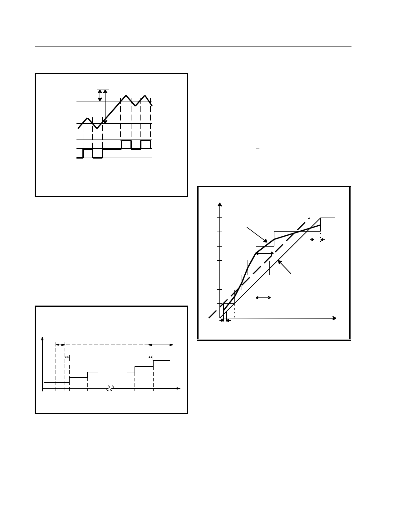
FIGURE 7. DNL MEASUREMENT ON PRODUCTION
TESTER
Analog
Input
DNL
LSB
Output
Codes
(N) Code Width = V(N+1) - V(N)
LSB = [ VREF(+) - VREF(-) ] / 1024
DNL(N) = [ V(N+1) - V(N) ] - LSB
V(N+1)
V(N)
N+1
N
N-1
Figure 8 shows the zero scale and full scale error
terms.
Figure 9 gives a visual definition of the INL error. The
chart shows a 3-bit converter transfer curve with
greatly exaggerated DNL errors to show the deviation
of the real transfer curve from the ideal one.
After a tester has measured all the transition voltag-
es, the computer draws a line parallel to the ideal
transfer line. By definition the best fit line makes
equal the positive and the negative INL errors. For ex-
ample, an INL error of -1 to +2 LSB's relative to the
Ideal Line would be +1.5 LSB's relative to the best fit
line.
FIGURE 9. INL ERROR CALCULATION
The formulas for Differential Non-Linearity (DNL), In-
tegral Non-Linearity (INL) and zero and full scale er-
rors (EZS, EFS) are:
DNL (001) = V002 - V001 - LSB
:::
DNL (3FE) = V3FF - V3FE - LSB
EFS (full scale error) = V3FF - [VREF(+) -1.5 * LSB]
EZS (zero scale error) = V001 - [VREF(-) + 0.5 * LSB]
FIGURE 8. REAL A/D TRANSFER CURVE
Output
Codes
7
Real Transfer Line
6
Best Fit Line
5
INL
4
EFS
3 Ideal Transfer Line
2
1 LSB
DIGITAL
CODES
0.5 ∗ LSB
EZS
002
001
000
VREF(-)
V001
V002
1.5 ∗ LSB
EFS
3FF
3FE
V3FE
V3FF
V
VREF(+)
Analog Input (Volt)
EZS
1.2 CLOCK AND CONVERSION TIMING
A system will clock the XRD8799 continuously or it
will give clock pulses intermittently when a conversion
is desired. The timing of Figure 10a shows normal
operation, while the timing of Figure 10b keeps the
XRD8799 in balance and ready to sample the analog
input.
11
11 Page | ||
| Páginas | Total 23 Páginas | |
| PDF Descargar | [ Datasheet XRD8799.PDF ] | |
Hoja de datos destacado
| Número de pieza | Descripción | Fabricantes |
| XRD8799 | A/D CONVERTER | Exar Corporation |
| Número de pieza | Descripción | Fabricantes |
| SLA6805M | High Voltage 3 phase Motor Driver IC. |
Sanken |
| SDC1742 | 12- and 14-Bit Hybrid Synchro / Resolver-to-Digital Converters. |
Analog Devices |
|
DataSheet.es es una pagina web que funciona como un repositorio de manuales o hoja de datos de muchos de los productos más populares, |
| DataSheet.es | 2020 | Privacy Policy | Contacto | Buscar |
