|
|
|
PDF 6225CA Data sheet ( Hoja de datos )
| Número de pieza | 6225CA | |
| Descripción | ISL6225CA | |
| Fabricantes | Intersil Corporation | |
| Logotipo | ||
Hay una vista previa y un enlace de descarga de 6225CA (archivo pdf) en la parte inferior de esta página. Total 18 Páginas | ||
|
No Preview Available !
www.DataSheet4U.com ®
Data Sheet
September 2003
ISL6225
FN9049.4
Dual Mobile-Friendly PWM Controller with
DDR Memory Option
The ISL6225 dual PWM controller delivers high efficiency and
tight regulation from two voltage regulating synchronous buck
DC/DC converters. The ISL6225 PWM power supply controller
was designed especially for DDR DRAM, SDRAM, and graphic
chipset applications in high performance desknote PCs,
notebook PCs, sub-notebook PCs, and PDAs.
Automatic mode selection of constant-frequency synchronous
rectification at heavy load, and hysteretic diode-emulation at
light load, assure high efficiency over a wide range of
conditions. The hysteretic mode of operation can be disabled
separately on each PWM converter if constant-frequency
continuous-conduction operation is desired for all load levels.
Efficiency is further enhanced by using the lower MOSFET
RDS(ON) as the current sense element.
Voltage-feed-forward ramp modulation, average current mode
control, and internal feedback compensation provide fast
response to input voltage and output load transients. Input
current ripple is minimized by channel to channel PWM
phase shift of 0°, 90°, or 180° determined by input voltage
and status of the DDR pin.
The ISL6225 can control two independent output voltages
adjustable from 0.9V to 5.5V or, by activating the DDR pin,
transform into a complete DDR memory power supply
solution. In DDR mode, CH2 output voltage VTT tracks CH1
output voltage VDDQ. CH2 output can both source and sink
current, an essential power supply feature for DDR memory
systems. The reference voltage VREF required by DDR
memory is generated as well.
In dual power supply applications the ISL6225 monitors the
output voltage of both CH1 and CH2. An independent
PGOOD (power good) signal is asserted for each channel
after the soft-start sequence has completed, and the output
voltage is within ±10% of the set point. In DDR mode CH1
generates the only PGOOD signal.
Built-in over-voltage protection prevents the output from
going above 115% of the set point by holding the lower
MOSFET on and the upper MOSFET off. When the output
voltage decays below the over-voltage threshold, normal
operation automatically resumes. Once the soft-start
sequence has completed, under-voltage protection may
latch the ISL6225 off if either output drops below 75% of its
set point value.
Adjustable over-current protection (OCP) monitors the
voltage drop across the RDS(ON) of the lower MOSFET. If
more precise current-sensing is required, an external current
sense resistor may be used.
Ordering Information
PART NUMBER TEMP. (oC) PACKAGE
PKG. NO.
ISL6225CA
-10 to 85
28 Ld SSOP
M28.15
ISL6225CA-T
-10 to 85 28 Ld SSOP Tape
and Reel
M28.15
Features
• Provides regulated output voltage in the range of 0.9V-5.5V
- High efficiency over wide load range
- Synchronous buck converter with hysteretic operation at
light load
- Inhibit Hysteretic mode on one, or both channels
• Complete DDR memory power solution
- VTT tracks VDDQ/2
- VDDQ/2 buffered reference output
• No current-sense resistor required
- Uses MOSFET RDS(ON)
- Optional current-sense resistor for precision Over-Current
• Under-voltage lock-out on VCC pin
• Dual input voltage mode operation
- Operates directly from battery 5V to 24V input
- Operates from 3.3V or 5V system rail
- VCC from 5V only
• Excellent dynamic response
- Combined voltage feed-forward and average current
mode control
• Power-good signal for each channel
• 300kHz switching frequency
- 180° channel to channel phase operation for reduced input
ripple when not in DDR mode
- 0° channel to channel phase operation in DDR mode for
reduced channel interference
- 90° channel to channel phase operation for reduced input
ripple in DDR mode when VIN is at GND.
Applications
• Mobile PCs
• PDAs
• Hand-held portable instruments
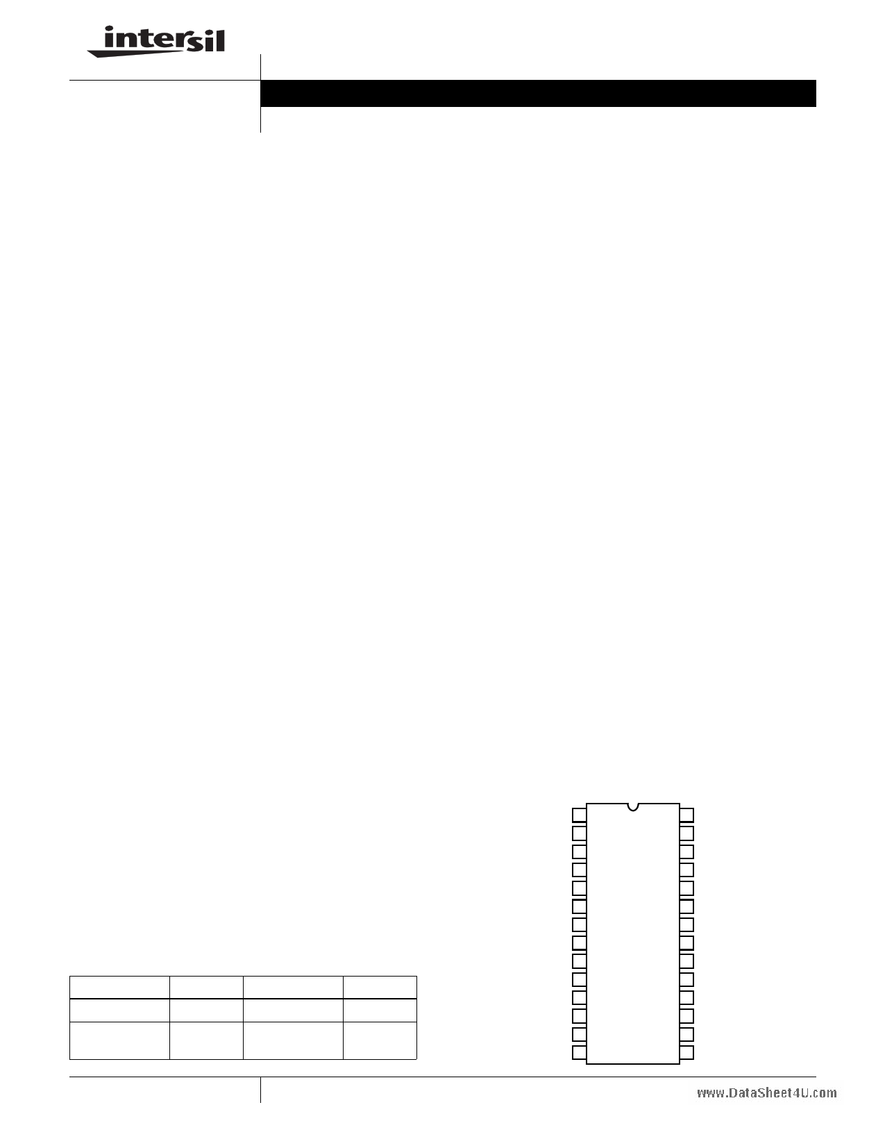
Pinout
ISL6225
SSOP-28
TOP VIEW
GND 1
28 VCC
LGATE1 2
27 LGATE2
PGND1 3
26 PGND2
PHASE1 4
25 PHASE2
UGATE1 5
24 UGATE2
BOOT1 6
23 BOOT2
ISEN1 7
22 ISEN2
EN1 8
21 EN2
VOUT1 9
20 VOUT2
VSEN1 10
19 VSEN2
OCSET1 11
18 OCSET2
SOFT1 12
17 SOFT2
DDR 13
16 PG2/REF
VIN 14
15 PG1
1
CAUTION: These devices are sensitive to electrostatic discharge; follow proper IC Handling Procedures.
1-888-INTERSIL or 321-724-7143 | Intersil (and design) is a registered trademark of Intersil Americas Inc.
Copyright © Intersil Americas Inc. 2003. All Rights Reserved
All other trademarks mentioned are the property of their respective owners.
1 page 
www.DataSheet4U.com
Generic Application Circuits
ISL6225
ENABLE OCSET1
+VIN
+3.3V TO +24V
+5V
EN1
EN2
VCC
DDR
OCSET2
PWM1
PWM2
Q1
L1
+
Q2 C1
VOUT1
+1.80V
Q3
L2
VOUT2
+1.20V
+
Q4 C2
FIGURE 1. ISL6225 APPLICATION CIRCUIT FOR TWO CHANNEL POWER SUPPLY
ENABLE OCSET1
+VIN
+3.3V TO +24V
+5V
EN1
EN2
VCC
DDR
PG2/VREF
PWM1
PWM2
Q1
L1
+
Q2 C1
VDDQ
+2.50V
OCSET2
Q3
L2
VTT
+1.25V
+
Q4 C2
VREF
+1.25V
FIGURE 2. ISL6225 APPLICATION CIRCUIT FOR COMPLETE DDR MEMORY POWER SUPPLY
5
5 Page 
www.DataSheet4U.com
ISL6225
If load step is strong enough to pull output voltage lower
than the Under-Voltage threshold, the chip shuts down
immediately.
Because of the nature of the used current sensing
technique, and to accommodate wide range of the RDS(ON)
variation, the value of the Over-Current threshold should
represent overload current about 150%...180% of the
nominal value. If more precise current protection is desired,
a current sense resistor placed in series with the lower
MOSFET source may be used.
Over-Voltage Protection
Should the output voltage increase over 115% of the normal
value due to the upper MOSFET failure, or other reasons,
the Over-Voltage protection comparator will force the
synchronous rectifier gate driver high. This action actively
pulls down the output voltage and eventually attempts to
blow the battery fuse. As soon as the output voltage drops
below the threshold, the OVP comparator is disengaged.
This OVP scheme provides a ‘soft’ crowbar function which
helps to tackle severe load transients and does not invert the
output voltage when activated -- a common problem for OVP
schemes with a latch.
Over-Temperature Protection
The chip incorporates an over-temperature protection circuit
that shuts the chip down when the die temperature of 150oC
is reached. Normal operation restores at die temperatures
below 125oC through the full soft-start cycle.
DDR Application
Double Data Rate (DDR) memory chips are expected to take
the place of traditional memory in many newly designed
computers, including high-end notebooks, due to increased
throughput. A novel feature associated with this type of
memory is new referencing and data bus termination
techniques. These techniques employ a reference voltage,
VREF, that tracks the center point of VDDQ and VSS
voltages and an additional VTT power source to which all
terminating resistors are connected. Despite the additional
power source, the overall memory power consumption is
reduced compared to traditional termination.
The added power source has a cluster of requirements that
should be observed and considered. Due to reduced
differential thresholds of DDR memory, the termination
power supply voltage, VTT, shall closely track VDDQ/2
voltage. Another very important feature for the termination
power supply is a capability to equally operate in sourcing
and sinking modes. The VTT supply shall regulate the output
voltage with the same degree of precision when current is
floating from the supply to the load and when the current is
diverted back from the load into the power supply. The last
mode of operation usually conflicts with the way most PWM
controllers operate.
The ISL6225 dual channel PWM controller possesses
several important means that allow re configuration for this
particular application and provide all three voltages required
in DDR memory compliant computer.
To reconfigure the ISL6225 for a complete DDR solution, the
DDR pin shall be permanently set high. The simplest way to
do that is to connect it to the VCC rail. This activates some
functions inside the chip that are specific to the DDR
memory power needs.
In DDR application presented in Figure 14 and 15, the first
controller regulates the VDDQ rail to 2.5V. The output
voltage is set by an external divider R3 and R5. The second
controller regulates the VTT rail to VDDQ/2. The OCSET2
pin function is now different. The pin serves now as an input
that brings VDDQ/2 voltage created by R4 and R6 divider
inside the chip. That effectively provides a tracking function
for the VTT voltage.
The PG2 pin function is also different in DDR mode. This pin
becomes the output of the buffer, which input is connected
via the OCSET2 pin to the center point of the R/R divider
from the VDDQ output. The buffer output voltage serves as
1.25V reference for the DDR memory chips. Current
capability of this pin is about 10mA.
For the VTT channel some control and protective functions
can be significantly simplified as this output is derived from
the VDDQ output. For example, the Over-Current and Over-
Voltage protections for the second controller are disabled
when the DDR pin is set high. The hysteretic mode of
operation is also disabled on the VTT channel to allow
sinking capability to be independent from the load level. As
the VTT channel tracks the VDDQ/2 voltage, the soft-start
function is not required and the SOFT2 pin may be left open.
Channel Synchronization in DDR
Applications
Presence of two PWM controllers on the same die require
channel synchronization to reduce inter channel interference
that may cause the duty factor jitter and increased output
ripple. The PWM controller is mostly susceptible to noise
when an error signal on the input of the PWM comparator
approaches the decision making point. False triggering can
occur causing jitter and affecting the output regulation.
Out-of-phase operation is a common approach to
synchronize dual channel converters as it reduces an input
current ripple and provides a minimum interference for
channels that control different voltage levels. When used in
DDR application with cascaded converters (VTT generated
from VDDQ), the turn-on of the upper MOSFET in the VDDQ
channel happens to be just before the decision making point
in the VTT channel that is running with a duty-factor close to
50%, as in Figure 10.
11
11 Page | ||
| Páginas | Total 18 Páginas | |
| PDF Descargar | [ Datasheet 6225CA.PDF ] | |
Hoja de datos destacado
| Número de pieza | Descripción | Fabricantes |
| 6225CA | ISL6225CA | Intersil Corporation |
| Número de pieza | Descripción | Fabricantes |
| SLA6805M | High Voltage 3 phase Motor Driver IC. |
Sanken |
| SDC1742 | 12- and 14-Bit Hybrid Synchro / Resolver-to-Digital Converters. |
Analog Devices |
|
DataSheet.es es una pagina web que funciona como un repositorio de manuales o hoja de datos de muchos de los productos más populares, |
| DataSheet.es | 2020 | Privacy Policy | Contacto | Buscar |