|
|
|
PDF CB664 Data sheet ( Hoja de datos )
| Número de pieza | CB664 | |
| Descripción | I2C Clock Distribution Buffer | |
| Fabricantes | Cypress Semiconductor | |
| Logotipo | ||
Hay una vista previa y un enlace de descarga de CB664 (archivo pdf) en la parte inferior de esta página. Total 8 Páginas | ||
|
No Preview Available !
www.DataSheet4U.com
CB664
I2C Clock Distribution Buffer for Three Banks of Mobile SDRAM
Approved Product
Product Features
• 7 output buffer for high clock fanout applications.
• Output may be individually disabled with I2C
• VDD = 3.3 volts
• Output frequency range 10 MHz to 100 MHz
• <250ps skew between output clocks.
• 16-pin SSOP and TSSOP package.
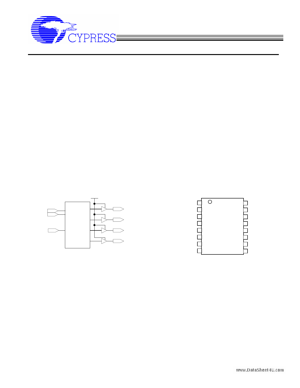
Block Diagram
SDATA
SCLK
REFIN
I2C Control
VDD
2
1
2
2
SDR(0:1)
SDR2
SDR(3:4)
SDR(5:6)
Product Description
The device is a high fanout system clock buffer. Its
primary application is to distribute clocks needed to
support a wide range of applications such as SDRAM
clocks. This device provides low skew distribution
clock heavily loaded. One important application of
this component is where long traces are used to
transport clocks from their generating devices to their
loads. The creation of EMI and the degradation of
waveform rise and fall times is greatly reduces by
running a single reference clock trace to this device
and then using it to these devices EMI is therefore
minimized and board real estate is saved.
Pin Configuration
VDD
SDR0
SDR1
VSS
CLKIN
SDR2
VDD
SDATA
1
2
3
4
5
6
7
8
16 SDR6
15 SDR5
14 VSS
13 VDD
12 SDR4
11 SDR3
10 VSS
9 SCLK
Cypress Semiconductor Corporation
525 Los Coches St.
Milpitas, CA 95035. Tel: 408-263-6300, Fax: 408-263-6571
http://www.cypress.com
Document#: 38-07024 Rev. **
5/6/99
Page 1 of 8
1 page 
www.DataSheet4U.com
CB664
I2C Clock Distribution Buffer for Three Banks of Mobile SDRAM
Approved Product
PCB Layout Suggestion
Via to VDD Plane
C1
1
2
3
4
5
6
C2 7
8
16
15
14
C3
13
12
11
10
9
FBI or R1
VCC
Via to GND Plane
Void (Cut) in power plane
C7
6.8 to 22µF
This is only a layout recommendation for best performance and lower EMI. The designer may choose a different
approach but C1, C2, C3 (all are o.1µF) should always be used and placed as close to their VDD pins as is
physically possible. FB1 or R1 is a ferrite Bead or resistor as needed to reduce conducted EMI from the device
into the systems power circuitry.
Cypress Semiconductor Corporation
525 Los Coches St.
Milpitas, CA 95035. Tel: 408-263-6300, Fax: 408-263-6571
http://www.cypress.com
Document#: 38-07024 Rev. **
5/6/99
Page 5 of 8
5 Page | ||
| Páginas | Total 8 Páginas | |
| PDF Descargar | [ Datasheet CB664.PDF ] | |
Hoja de datos destacado
| Número de pieza | Descripción | Fabricantes |
| CB664 | I2C Clock Distribution Buffer | Cypress Semiconductor |
| Número de pieza | Descripción | Fabricantes |
| SLA6805M | High Voltage 3 phase Motor Driver IC. |
Sanken |
| SDC1742 | 12- and 14-Bit Hybrid Synchro / Resolver-to-Digital Converters. |
Analog Devices |
|
DataSheet.es es una pagina web que funciona como un repositorio de manuales o hoja de datos de muchos de los productos más populares, |
| DataSheet.es | 2020 | Privacy Policy | Contacto | Buscar |