|
|
|
PDF XR16V794 Data sheet ( Hoja de datos )
| Número de pieza | XR16V794 | |
| Descripción | HIGH PERFORMANCE 2.25V TO 3.6V QUAD UART | |
| Fabricantes | Exar Corporation | |
| Logotipo | ||
Hay una vista previa y un enlace de descarga de XR16V794 (archivo pdf) en la parte inferior de esta página. Total 30 Páginas | ||
|
No Preview Available !
www.DataSheet4U.com
XR16V794
HIGH PERFORMANCE 2.25V TO 3.6V QUAD UART WITH FRACTIONAL
MAY 2007
REV. 1.0.0
GENERAL DESCRIPTION
The XR16V7941 (794), is a 2.25V to 3.6V octal
Universal Asynchronous Receiver and Transmitter
(UART) with 5V tolerant serial (modem) inputs. The
highly integrated device is designed for high
bandwidth requirement in communication systems.
The global interrupt source register provides a
complete interrupt status indication for all 4 channels
to speed up interrupt parsing. Each UART has its own
16C550 compatible set of configuration registers, TX
and RX FIFOs of 64 bytes, fully programmable
transmit and receive FIFO trigger levels, TX and RX
FIFO level counters, automatic RTS/CTS or DTR/
DSR hardware flow control with programmable
hysteresis, autoamtic software (Xon/Xoff) flow
control, RS-485 half-duplex direction control with
programmable turn-around delay, Intel or Motorola
bus interface and sleep mode with a wake-up
indicator.
NOTE: Covered by US patents #5,649,122 and #5,949,787
APPLICATIONS
• Remote Access Servers
• Ethernet Network to Serial Ports
• Network Management
• Factory Automation and Process Control
• Point-of-Sale Systems
• Multi-port RS-232/RS-422/RS-485 Cards
FEATURES
• 2.25V to 3.6V with 5V Tolerant Serial Inputs
• Single Interrupt output for all 4 UARTs
• A Global Interrupt Source Register for all 4 UARTs
• 5G “Flat” UART Registers for easier programming
• Simultaneous Initialization of all UART channels
• A General Purpose Command-driven 16-bit
Timer/counter
• Sleep Mode with Wake-up Indication
• Highly Integrated Device for Space Saving
• Each UART is independently controlled with:
■ 16C550 Compatible 5G Register Set
■ 64-byte Transmit and Receive FIFOs
■ Fractional Baud Rate Generator
■ Transmit and Receive FIFO Level Counters
■ Programmable TX and RX FIFO Trigger Level
■ Automatic RTS/CTS or DTR/DSR Flow Control
■ Automatic Xon/Xoff Software Flow Control
■ RS485 Half-Duplex Control Output with
Selectable Turn-around Delay
■ Infrared (IrDA 1.0) Data Encoder/Decoder
■ Programmable Data Rate with Prescaler
• Up to 8 Mbps Serial Data Rate
• Pin compatible to XR16L784. Same 64-pin LQFP
Package (10x10x1.4 mm)
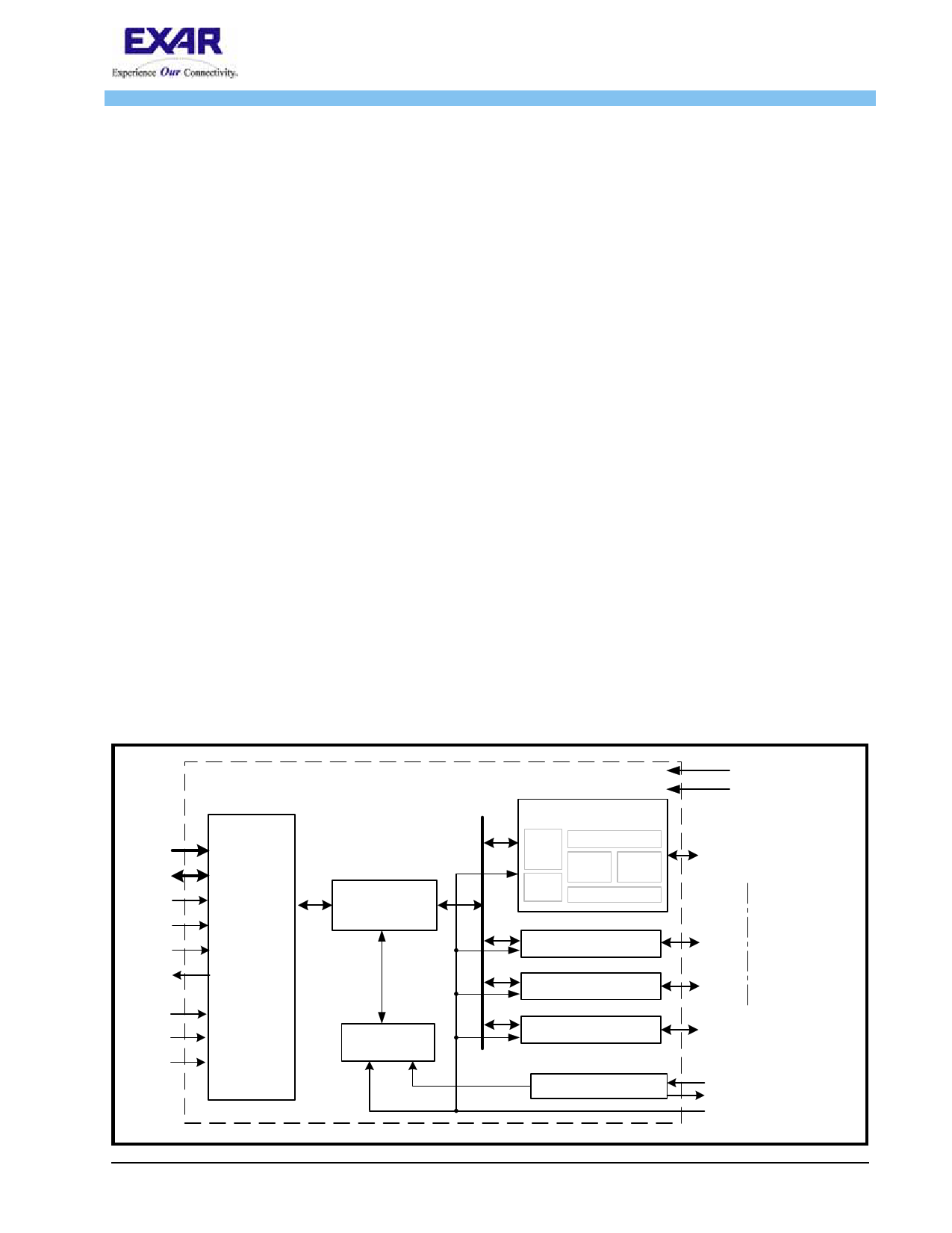
FIGURE 1. BLOCK DIAGRAM
A7:A0
D7:D0
IOR#
IOW#
CS#
INT#
16/68#
RST#
ENIR
Intel or
Motorola
Data
Bus
Interface
Device
Configuration
Register
s
16-bit
Timer/Counter
*All Inputs are 5V Tolerant
(Except XTAL1)
UART Channel 0
UART
Regs
BRG
64 Byte TX FIFO
TX &
RX
IR
ENDEC
64 Byte RX FIFO
UART Channel 1
UART Channel 2
UART Channel 3
Crystal Osc/
Buffer
2.25V to 3.6V VCC
GND
TX0, RX0, DTR0#,
DSR0#, RTS0#,
CTS0#, CD0#, RI0#
TX3, RX3, DTR3#,
DSR3#, RTS3#,
CTS3#, CD3#, RI3#
XTAL1
XTAL2
TMRCK
Exar Corporation 48720 Kato Road, Fremont CA, 94538 • (510) 668-7000 • FAX (510) 668-7017 • www.exar.com
1 page 
REV. 1.0.0
XR16V794
HIGH PERFORMANCE 2.25V TO 3.6V QUAD UART WITH FRACTIONAL BAUD RATE
NAME
TX3
RX3
PIN #
28
21
RTS3#
26
CTS3#
22
DTR3#
27
DSR3#
23
CD3#
24
RI3#
25
ANCILLARY SIGNALS
XTAL1
50
XTAL2
49
TMRCK
31
ENIR
32
RST#
16/68#
20
19
VCC
GND
9,30,52
10,29,51
TYPE
DESCRIPTION
O UART channel 3 Transmit Data or infrared transmit data. Normal TXD output idles
HIGH while infrared TXD output idles LOW.
I UART channel 3 Receive Data or infrared receive data. Normal RXD input idles
HIGH while infrared RXD input idles LOW. In the infrared mode, the polarity of the
incoming RXD signal can be selected via FCTR bit-4. If this bit is a logic 0, a LOW
on the RXD input is considered a mark and if this bit is a logic 1, a HIGH on the
RXD input is considered a space.
O UART channel 3 Request to Send or general purpose output (active low). See
description of RTS0# pin.
I UART channel 3 Clear to Send or general purpose input (active low).d. See
description of CTS0# pin.
O UART channel 3 Data Terminal Ready or general purpose output (active low). See
description of DTS0# pin.
I UART channel 3 Data Set Ready or general purpose input (active low). See
description of DSR0# pin.
I UART channel 3 Carrier Detect or general purpose input (active low).
I UART channel 3 Ring Indicator or general purpose input (active low).
I Crystal or external clock input. Caution: this input is not 5V tolerant.
O Crystal or buffered clock output.
I 16-bit timer/counter external clock input.
I Infrared mode enable (active high). This pin is sampled during power up, following
a hardware reset (RST#) or soft-reset (register RESET). It can be used to start up
all 4 UARTs in the infrared mode. The sampled logic state is transferred to MCR bit-
6 in the UART.
I Reset (active low). The configuration and UART registers are reset to default val-
ues, see Table 19.
I Intel or Motorola data bus interface select. HIGH selects Intel bus interface and
LOW selects Motorola interface. This input affects the functionality of IOR#, IOW#
and CS# pins.
+2.25V to 3.6V supply with 5V tolerant serial (modem) inputs.
Power supply common, ground.
NOTE: Pin type: I=Input, O=Output, IO= Input/output, OD=Output Open Drain.
5
5 Page 
XR16V794
REV. 1.0.0
HIGH PERFORMANCE 2.25V TO 3.6V QUAD UART WITH FRACTIONAL BAUD RATE
2.8 Receiver
The receiver section contains an 8-bit Receive Shift Register (RSR) and 64 bytes of FIFO which includes a
byte-wide Receive Holding Register (RHR). The RSR uses the 16X (or the 8X) clock for timing. It verifies and
validates every bit on the incoming character in the middle of each data bit. On the falling edge of a start or
false start bit, an internal receiver counter starts counting the number of 16X (or 8X) clocks. After 8 (or 4)
clocks the start bit period should be at the center of the start bit. At this time the start bit is sampled and if it is
still a logic 0 it is validated. Evaluating the start bit in this manner prevents the receiver from assembling a false
character. The rest of the data bits and stop bits are sampled and validated in this same manner to prevent
false framing. If there were any error(s), they are reported in the LSR register bits 2-4. Upon unloading the
receive data byte from RHR, the receive FIFO pointer is bumped and the error tags are immediately updated to
reflect the status of the data byte in RHR register. RHR can generate a receive data ready interrupt upon
receiving a character or delay until it reaches the FIFO trigger level. Furthermore, data delivery to the host is
guaranteed by a receive data ready time-out interrupt when data is not received for 4 word lengths as defined
by LCR[1:0] plus 12 bits time. This is equivalent to 3.7-4.6 character times. The RHR interrupt is enabled by
IER bit-0.
2.8.1 Receive Holding Register (RHR) - Read-Only
The Receive Holding Register is an 8-bit register that holds a receive data byte from the Receive Shift
Register. It provides the receive data interface to the host processor. The RHR register is part of the receive
FIFO of 64 bytes by 11-bits wide, the 3 extra bits are for the 3 error tags to be reported in LSR register. When
the FIFO is enabled by FCR bit-0, the RHR contains the first data character received by the FIFO. After the
RHR is read, the next character byte is loaded into the RHR and the errors associated with the current data
byte are immediately updated in the LSR bits 2-4.
FIGURE 7. RECEIVER OPERATION IN NON-FIFO MODE
16X or 8X Clock
Receive Data Shift
Register (RSR)
Data Bit
Validation
Receive Data Characters
Receive
Data Byte
and Errors
Error
Tags in
LSR bits
4:2
Receive Data
Holding Register
(RHR)
RHR Interrupt (ISR bit-2)
RXFIFO1
11
11 Page | ||
| Páginas | Total 30 Páginas | |
| PDF Descargar | [ Datasheet XR16V794.PDF ] | |
Hoja de datos destacado
| Número de pieza | Descripción | Fabricantes |
| XR16V794 | HIGH PERFORMANCE 2.25V TO 3.6V QUAD UART | Exar Corporation |
| XR16V798 | HIGH PERFORMANCE 2.25V TO 3.6V OCTAL UART | Exar Corporation |
| Número de pieza | Descripción | Fabricantes |
| SLA6805M | High Voltage 3 phase Motor Driver IC. |
Sanken |
| SDC1742 | 12- and 14-Bit Hybrid Synchro / Resolver-to-Digital Converters. |
Analog Devices |
|
DataSheet.es es una pagina web que funciona como un repositorio de manuales o hoja de datos de muchos de los productos más populares, |
| DataSheet.es | 2020 | Privacy Policy | Contacto | Buscar |