|
|
|
PDF NCP1200P100 Data sheet ( Hoja de datos )
| Número de pieza | NCP1200P100 | |
| Descripción | PWM Current-Mode Controller for Low-Power Universal Off-Line Supplies | |
| Fabricantes | ON Semiconductor | |
| Logotipo | ||
Hay una vista previa y un enlace de descarga de NCP1200P100 (archivo pdf) en la parte inferior de esta página. Total 16 Páginas | ||
|
No Preview Available !
NCP1200
PWM Current−Mode
Controller for Low−Power
Universal Off−Line Supplies
Housed in SOIC−8 or PDIP−8 package, the NCP1200 represents a
major leap toward ultra−compact Switchmode Power Supplies. Due to
a novel concept, the circuit allows the implementation of a complete
offline battery charger or a standby SMPS with few external
components. Furthermore, an integrated output short−circuit
protection lets the designer build an extremely low−cost AC−DC wall
adapter associated with a simplified feedback scheme.
With an internal structure operating at a fixed 40 kHz, 60 kHz or
100 kHz, the controller drives low gate−charge switching devices like
an IGBT or a MOSFET thus requiring a very small operating power.
Due to current−mode control, the NCP1200 drastically simplifies the
design of reliable and cheap offline converters with extremely low
acoustic generation and inherent pulse−by−pulse control.
When the current setpoint falls below a given value, e.g. the output
power demand diminishes, the IC automatically enters the skip cycle
mode and provides excellent efficiency at light loads. Because this
occurs at low peak current, no acoustic noise takes place.
Finally, the IC is self−supplied from the DC rail, eliminating the
need of an auxiliary winding. This feature ensures operation in
presence of low output voltage or shorts.
Features
• No Auxiliary Winding Operation
• Internal Output Short−Circuit Protection
• Extremely Low No−Load Standby Power
• Current−Mode with Skip−Cycle Capability
• Internal Leading Edge Blanking
• 250 mA Peak Current Source/Sink Capability
• Internally Fixed Frequency at 40 kHz, 60 kHz and 100 kHz
• Direct Optocoupler Connection
• Built−in Frequency Jittering for Lower EMI
• SPICE Models Available for TRANsient and AC Analysis
• Internal Temperature Shutdown
• Pb−Free Packages are Available
Typical Applications
• AC−DC Adapters
• Offline Battery Chargers
• Auxiliary/Ancillary Power Supplies (USB, Appliances, TVs, etc.)
http://onsemi.com
8
1
8
1
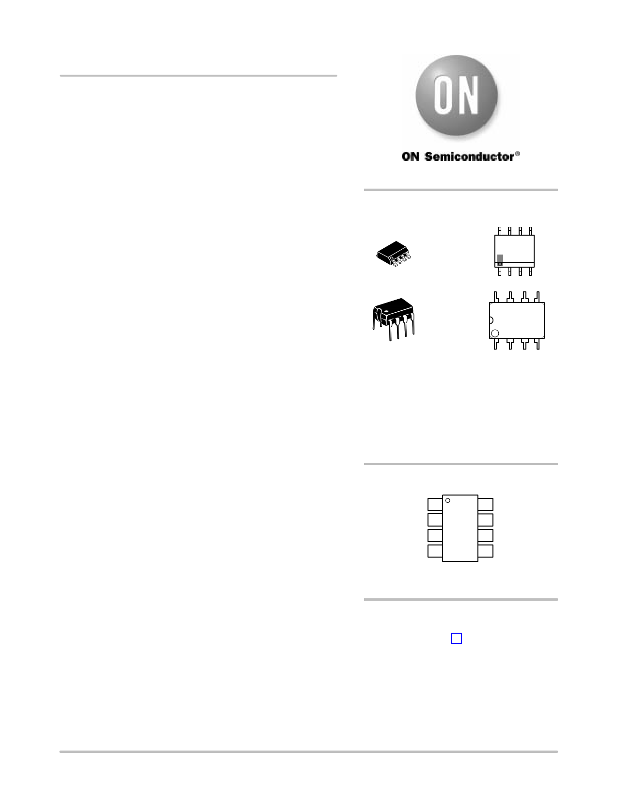
SOIC−8
D SUFFIX
CASE 751
PDIP−8
P SUFFIX
CASE 626
MARKING
DIAGRAMS
8
200Dy
ALYW
1
8
1200Pxxx
AWL
YYWW
1
xxx = Device Code: 40, 60 or 100
y = Device Code:
4 for 40
6 for 60
1 for 100
A = Assembly Location
L = Wafer Lot
Y, YY = Year
W, WW = Work Week
PIN CONNECTIONS
Adj 1
FB 2
CS 3
GND 4
8 HV
7 NC
6 VCC
5 Drv
(Top View)
ORDERING INFORMATION
See detailed ordering and shipping information in the package
dimensions section on page 14 of this data sheet.
© Semiconductor Components Industries, LLC, 2004
December, 2004 − Rev. 13
1
Publication Order Number:
NCP1200/D
1 page 
NCP1200
60 11.70
50 11.60
40 11.50
30 11.40
20 11.30
10 11.20
0
−25 0
25 50 75 100
TEMPERATURE (°C)
Figure 3. HV Pin Leakage Current vs.
Temperature
11.10
125 −25
100 kHz
60 kHz
40 kHz
0 25 50 75 100
TEMPERATURE (°C)
Figure 4. VCC OFF vs. Temperature
125
9.85
9.80
9.75
9.70
9.65
9.60
9.55
9.50
9.45
−25
100 kHz
60 kHz
900
850
800
40 kHz
750 100 kHz
700
60 kHz
650
40 kHz
600
0 25 50 75 100 125
−25 0
25 50 75 100 125
TEMPERATURE (°C)
TEMPERATURE (°C)
Figure 5. VCC ON vs. Temperature
Figure 6. ICC1 vs. Temperature
2.10
1.90
1.70
1.50
1.30
1.10
0.90
−25
110
100 kHz
104
98 100 kHz
92
86
80
60 kHz
74
68 60 kHz
62
40 kHz
56
50 40 kHz
44
38
0 25 50 75 100 125
−25 0
25 50 75 100 125
TEMPERATURE (°C)
TEMPERATURE (°C)
Figure 7. ICC2 vs. Temperature
Figure 8. Switching Frequency vs. TJ
http://onsemi.com
5
5 Page 
NCP1200
Figure 21. A negative spike takes place on the Bulk capacitor at the switch−off sequence
Simple and inexpensive cures exist to prevent from
internal parasitic SCR activation. One of them consists in
inserting a resistor in series with the high−voltage pin to
keep the negative current to the lowest when the bulk
becomes negative (Figure 22). Please note that the negative
spike is clamped to –2 x Vf due to the diode bridge. Please
refer to AND8069/D for power dissipation calculations.
Another option (Figure 23) consists in wiring a diode from
VCC to the bulk capacitor to force VCC to reach UVLOlow
sooner and thus stops the switching activity before the bulk
capacitor gets deeply discharged. For security reasons, two
diodes can be connected in series.
+
Cbulk
1
2
3
4
3
Rbulk
> 4.7 k
2
8
7
6
5
1+
CVCC
+
Cbulk
1
2
3
4
3
8 D3
7 1N4007
6
5
1+
CVCC
Figure 22. A simple resistor in series avoids any
latchup in the controller
A Typical Application
Figure 24 depicts a low−cost 3.5 W AC−DC 6.5 V wall
adapter. This is a typical application where the wall−pack
must deliver a raw DC level to a given internally regulated
apparatus: toys, calculators, CD players etc. Due to the
Figure 23. or a diode forces VCC to reach
UVLOlow sooner
inherent short−circuit protection of the NCP1200, you only
need a bunch of components around the IC, keeping the final
cost at an extremely low level. The transformer is available
from different suppliers as detailed on the following page.
http://onsemi.com
11
11 Page | ||
| Páginas | Total 16 Páginas | |
| PDF Descargar | [ Datasheet NCP1200P100.PDF ] | |
Hoja de datos destacado
| Número de pieza | Descripción | Fabricantes |
| NCP1200P100 | PWM Current-Mode Controller for Low-Power Universal Off-Line Supplies | ON Semiconductor |
| Número de pieza | Descripción | Fabricantes |
| SLA6805M | High Voltage 3 phase Motor Driver IC. |
Sanken |
| SDC1742 | 12- and 14-Bit Hybrid Synchro / Resolver-to-Digital Converters. |
Analog Devices |
|
DataSheet.es es una pagina web que funciona como un repositorio de manuales o hoja de datos de muchos de los productos más populares, |
| DataSheet.es | 2020 | Privacy Policy | Contacto | Buscar |