|
|
|
PDF VRS51L580 Data sheet ( Hoja de datos )
| Número de pieza | VRS51L580 | |
| Descripción | (VRS51X570 / VRS51X580) Versa 8051 MCUs | |
| Fabricantes | Ramtron | |
| Logotipo | ||
Hay una vista previa y un enlace de descarga de VRS51L580 (archivo pdf) en la parte inferior de esta página. Total 30 Páginas | ||
|
No Preview Available !
www.DataSheet4U.com
VRS51x570/580
Datasheet
Rev 1.2
Versa 8051 MCUs with 32/64KB
Overview
The VRS51x570 and the VRS51x580 are low cost 8-bit
microcontrollers based on the standard 80C51
microcontroller family architecture. They are pin
compatible and drop-in replacements for most 8051
MCUs.
Ideal for a wide range of applications requiring large
amounts of program/data memory, coupled with
comprehensive peripheral support, the VRS51x570/580
devices include 32KB/64KB of Flash memory,
respectively, and 1KB of SRAM, 5 PWM output
channels, a UART, three 16-bit timers, a Watch Dog
timer and power down features.
These devices also include a fifth, 4-bit, I/O port mapped
into the “no connect” pins of the standard 8051/52
package. This provides a total of 36 I/Os while
maintaining compatibility with standard 80C51/52 pin
outs.
The VRS51x570 and VRS51x580 are available in
PLCC-44, QFP-44 and DIP-40 packages in the Industrial
temperature range. The Flash memory can be
programmed using programmers from Ramtron or other
3rd party commercial programmer suppliers.
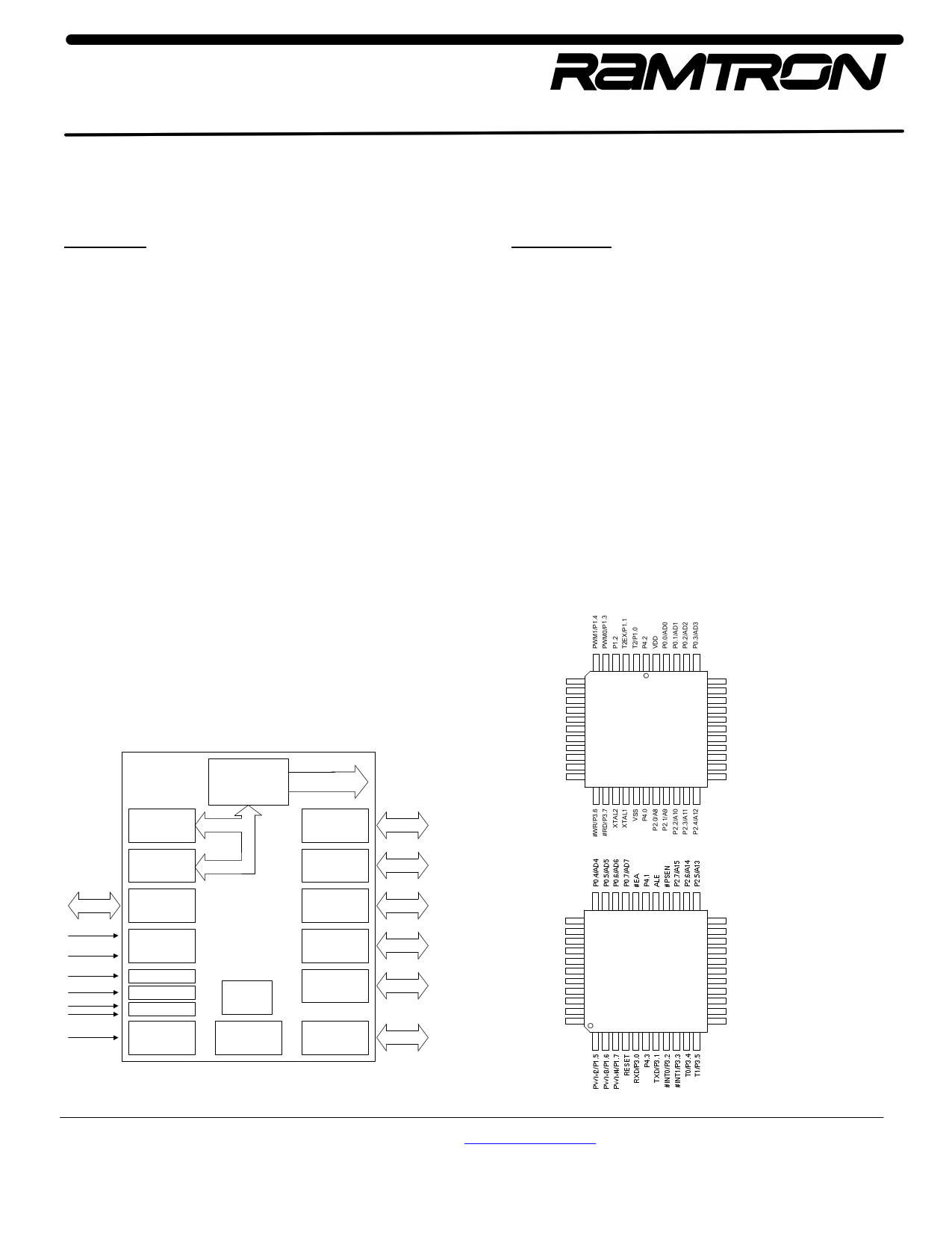
FIGURE 1: VRS51X570 / VRS51X580 FUNCTIONAL DIAGRAM
64KB
FLASH
1024 Bytes of
RAM
UART
2 INTERRUPT
INPUTS
TIMER 0
TIMER 1
TIMER 2
RESET
8051
PROCESSOR
ADDRESS/
DATA BUS
PORT 0
PORT 1
PORT 2
PORT 3
POWER
CONTROL
WATCHDOG
TIMER
PORT 4
PWM
8
8
8
8
4
5
Feature Set
• 80C51/80C52 pin compatible
• 12 clock periods per machine cycle
• 32KB / 64KB on-chip Flash memory
• 1024 Bytes on-chip data RAM
• 36 I/O lines: P0-P3 = 8-bit, P4 = 4-bit
• 5-Channel PWM on P1.3 to P1.7
• Full duplex serial port (UART)
• Three 16-bit Timers/Counters
• Watch Dog Timer
• 8-bit Unsigned Division / Multiply
• BCD arithmetic
• Direct and Indirect Addressing
• Two levels of interrupt priority and nested interrupts
• Power saving modes
• Code protection function
• Operates at a clock frequency of up to 40MHz
• Low EMI (inhibit ALE)
• Programming voltage: 12V
• Industrial Temperature range (-40°C to +85°C)
• 5V and 3V versions available (see Ordering information.)
FIGURE 2: VRS51X570 / VRS51X580 PLCC AND QFP PINOUT DIAGRAMS
PWM2/P1.5
PWM3/P1.6
PWM4/P1.7
RESET
RXD/P3.0
P4.3
TXD/P3.1
#INT0/P3.2
#INT1/P3.3
T0/P3.4
T1/P3.5
6
7
1
40
39
VRS51x570/580
PLCC -4 4
17 29
18 28
P0.4/AD4
P0.5/AD5
P0.6/AD6
P0.7/AD7
#EA
P4.1
ALE
#PSEN
P2.7/A15
P2.6/A14
P2.5/A13
P0.3/AD3
P0.2/AD2
P0.1/AD1
P0.0/AD0
VDD
P4.2
T2/P1.0
T2EX/P1.1
P1.2
PWM0/P1.3
PWM1/P1.4
33
34
23
22
VRS51x570/580
QFP-44
44 12
1 11
P2.4/A12
P2.3/A11
P2.2/A10
P2.1/A9
P2.0/A8
P4.0
VSS
XTAL1
XTAL2
#RD/P3.7
#WR/P3.6
Ramtron International Corporation ? http://www.ramtron.com
1850 Ramtron Drive Colorado Springs ? MCU customer service: 1-800-943-4625, 1-514-871-2447, ext. 208
Colorado, USA, 80921 ? 1-800-545-FRAM, 1-719-481-7000
page 1 of 49
1 page 
VRS51x570/580
Instruction Set
The following tables describe the instruction set of the
VRS51x570 and VRS51x580 devices. The instructions are
functional and binary code compatible with industry
standard 8051s.
TABLE 4: LEGEND FOR INSTRUCTION SET TABLE
Symbol
A
Rn
Direct
@Ri
rel
bit
#data
#data 16
addr 16
addr 11
Function
Accumulator
Register R0-R7
Internal register address
Internal register pointed to by R0 or R1 (except MOVX)
Two's complement offset byte
Direct bit address
8-bit constant
16-bit constant
16-bit destination address
11-bit destination address
TABLE 5: VRS51X570/VRS51X580 INSTRUCTION SET
Mnemonic
Description
Arithmetic instructions
ADD A, Rn
Add register to A
ADD A, direct
Add direct byte to A
ADD A, @Ri
Add data memory to A
ADD A, #data
Add immediate to A
ADDC A, Rn
Add register to A with carry
ADDC A, direct
Add direct byte to A with carry
ADDC A, @Ri
Add data memory to A with carry
ADDC A, #data
Add immediate to A with carry
SUBB A, Rn
Subtract register from A with borrow
SUBB A, direct
Subtract direct byte from A with borrow
SUBB A, @Ri
Subtract data mem from A with borrow
SUBB A, #data
Subtract immediate from A with borrow
INC A
Increment A
INC Rn
Increment register
INC direct
Increment direct byte
INC @Ri
Increment data memory
DEC A
Decrement A
DEC Rn
Decrement register
DEC direct
Decrement direct byte
DEC @Ri
Decrement data memory
INC DPTR
Increment data pointer
MUL AB
Multiply A by B
DIV AB
Divide A by B
DA A
Decimal adjust A
Logical Instructions
ANL A, Rn
AND register to A
ANL A, direct
AND direct byte to A
ANL A, @Ri
AND data memory to A
ANL A, #data
AND immediate to A
ANL direct, A
AND A to direct byte
ANL direct, #data AND immediate data to direct byte
ORL A, Rn
OR register to A
ORL A, direct
OR direct byte to A
ORL A, @Ri
OR data memory to A
ORL A, #data
OR immediate to A
ORL direct, A
OR A to direct byte
ORL direct, #data OR immediate data to direct byte
XRL A, Rn
Exclusive-OR register to A
XRL A, direct
Exclusive-OR direct byte to A
XRL A, @Ri
Exclusive-OR data memory to A
XRL A, #data
Exclusive-OR immediate to A
XRL direct, A
Exclusive-OR A to direct byte
XRL direct, #data Exclusive-OR immediate to direct byte
CLR A
Clear A
CPL A
Compliment A
SWAP A
Swap nibbles of A
RL A
Rotate A left
RLC A
Rotate A left through carry
RR A
Rotate A right
RRC A
Rotate A right through carry
Size
(bytes)
1
2
1
2
1
2
1
2
1
2
1
2
1
1
2
1
1
1
2
1
1
1
1
1
1
2
1
2
2
3
1
2
1
2
2
3
1
2
1
2
2
3
1
1
1
1
1
1
1
Instr. Cycles
1
1
1
1
1
1
1
1
1
1
1
1
1
1
1
1
1
1
1
1
2
4
4
1
1
1
1
1
1
2
1
1
1
1
1
2
1
1
1
1
1
2
1
1
1
1
1
1
1
Mnemonic
Description
Boolean Instruction
CLR C
Clear Carry bit
CLR bit
Clear bit
SETB C
Set Carry bit to 1
SETB bit
Set bit to 1
CPL C
Complement Carry bit
CPL bit
Complement bit
ANL C,bit
Logical AND between Carry and bit
ANL C,#bit
Logical AND between Carry and not bit
ORL C,bit
Logical ORL between Carry and bit
ORL C,#bit
Logical ORL between Carry and not bit
MOV C,bit
Copy bit value into Carry
MOV bit,C
Copy Carry value into Bit
Data Transfer Instructions
MOV A, Rn
Move register to A
MOV A, direct
Move direct byte to A
MOV A, @Ri
Move data memory to A
MOV A, #data
Move immediate to A
MOV Rn, A
Move A to register
MOV Rn, direct
Move direct byte to register
MOV Rn, #data
Move immediate to register
MOV direct, A
Move A to direct byte
MOV direct, Rn
Move register to direct byte
MOV direct, direct Move direct byte to direct byte
MOV direct, @Ri
Move data memory to direct byte
MOV direct, #data Move immediate to direct byte
MOV @Ri, A
Move A to data memory
MOV @Ri, direct
Move direct byte to data memory
MOV @Ri, #data
Move immediate to data memory
MOV DPTR, #data Move immediate to data pointer
MOVC A, @A+DPTR
Move code byte relative DPTR to A
MOVC A, @A+PC Move code byte relative PC to A
MOVX A, @Ri
Move external data (A8) to A
MOVX A, @DPTR Move external data (A16) to A
MOVX @Ri, A
Move A to external data (A8)
MOVX @DPTR, A Move A to external data (A16)
PUSH direct
Push direct byte onto stack
POP direct
Pop direct byte from stack
XCH A, Rn
Exchange A and register
XCH A, direct
Exchange A and direct byte
XCH A, @Ri
Exchange A and data memory
XCHD A, @Ri
Exchange A and data memory nibble
Branching Instructions
ACALL addr 11
Absolute call to subroutine
LCALL addr 16
Long call to subroutine
RET
Return from subroutine
RETI
Return from interrupt
AJMP addr 11
Absolute jump unconditional
LJMP addr 16
Long jump unconditional
SJMP rel
Short jump (relative address)
JC rel
Jump on carry = 1
JNC rel
Jump on carry = 0
JB bit, rel
Jump on direct bit = 1
JNB bit, rel
Jump on direct bit = 0
JBC bit, rel
Jump on direct bit = 1 and clear
JMP @A+DPTR
Jump indirect relative DPTR
JZ rel
Jump on accumulator = 0
JNZ rel
Jump on accumulator 1= 0
CJNE A, direct, rel
Compare A, direct JNE relative
CJNE A, #d, rel
Compare A, immediate JNE relative
CJNE Rn, #d, rel
Compare reg, immediate JNE relative
CJNE @Ri, #d, rel Compare ind, immediate JNE relative
DJNZ Rn, rel
Decrement register, JNZ relative
DJNZ direct, rel
Decrement direct byte, JNZ relative
Miscellaneous Instruction
NOP
No operation
Rn: Any of the register R0 to R7
@Ri: Indirect addressing using Register R0 or R1
#data: immediate Data provided with Instruction
#data16: Immediate data included with instruction
bit: address at the bit level
rel: relative address to Program counter from +127 to –128
Addr11: 11-bit address range
Addr16: 16-bit address range
#d: Immediate Data supplied with instruction
Size
(bytes)
1
2
1
2
1
2
2
2
2
2
2
2
1
2
1
2
1
2
2
2
2
3
2
3
1
2
2
3
1
1
1
1
1
1
2
2
1
2
1
1
2
3
1
1
2
3
2
2
2
3
3
3
1
2
2
3
3
3
3
2
3
1
Instr. Cycles
1
1
1
1
1
1
2
2
2
2
1
2
1
1
1
1
1
2
1
1
2
2
2
2
1
2
1
2
2
2
2
2
2
2
2
2
1
1
1
1
2
2
2
2
2
2
2
2
2
2
2
2
2
2
2
2
2
2
2
2
2
1
________________________________________________________________________________________________
www.ramtron.com
page 5 of 49
5 Page 
VRS51x570/580
Input/Output Ports
The VRS51x570 and VRS51x580 have a total of 36 bi-
directional I/O lines grouped into four 8-bit I/O ports
and one 4-bit I/O port. These I/Os can be individually
configured as inputs or outputs.
With the exception of the P0 I/Os, which are of the
open drain type, each I/O is made of a transistor
connected to ground and a weak pull-up resistor.
Writing a 0 in a given I/O port bit register will activate
the transistor connected to Vss and bring the I/O to a
LOW level.
Writing a 1 into a given I/O port bit register de-activates
the transistor between the pin and ground. In this case
the pull-up resistor will bring the corresponding pin to a
HIGH level.
To use a given I/O as an input, a 1 must be written into
its associated port register bit. By default, upon reset
all I/Os are configured as inputs.
General Structure of an I/O Port
The following elements establish the link between the
core unit and the pins of the microcontroller:
• Special Function Register (same name as port)
• Output Stage Amplifier (the structure of this
element varies with its auxiliary function)
From the following figure, one can see that the D flip-
flop stores the value received from the internal bus
after receiving a write signal from the core. Also, note
that the Q output of the flip-flop can be linked to the
internal bus by executing a read instruction.
This is how one would read the content of the register.
It is also possible to link the value of the pin to the
internal bus. This is done by the “read pin” instruction.
In short, the user may read the value of the register or
the pin.
FIGURE 6: INTERNAL STRUCTURE OF ONE OF THE EIGHT I/O PORT LINES
Read Register
Internal Bus
Write to
Register
Q
D Flip-Flop
Q
Output
Stage
IC Pin
Read Pin
Structure of the P1, P2, P3 and P4
The following figure provides a general idea of the
structure of the P1, P2, P3 and P4 ports. Note that the
intermediary logic that connects the output of the
register and the output stage together is not shown
because this logic varies with the auxiliary function of
each port.
FIGURE 7: GENERAL STRUCTURE OF THE OUTPUT STAGE OF P1, P2 AND P3
Read Register
Internal Bus
Write to
Register
Q
D Flip-Flop
Q
Vcc
Pull-up
Network
X1
IC Pin
Read Pin
Each line may be used independently as a logical
input or output. When used as an input, as mentioned
earlier, the corresponding port register bit must be
high.
Structure of Port 0
The internal structure of P0 is shown below. The
auxiliary function of this port requires a particular logic.
______________________________________________________________________________________________
www.ramtron.com
page 11 of 49
11 Page | ||
| Páginas | Total 30 Páginas | |
| PDF Descargar | [ Datasheet VRS51L580.PDF ] | |
Hoja de datos destacado
| Número de pieza | Descripción | Fabricantes |
| VRS51L580 | (VRS51X570 / VRS51X580) Versa 8051 MCUs | Ramtron |
| Número de pieza | Descripción | Fabricantes |
| SLA6805M | High Voltage 3 phase Motor Driver IC. |
Sanken |
| SDC1742 | 12- and 14-Bit Hybrid Synchro / Resolver-to-Digital Converters. |
Analog Devices |
|
DataSheet.es es una pagina web que funciona como un repositorio de manuales o hoja de datos de muchos de los productos más populares, |
| DataSheet.es | 2020 | Privacy Policy | Contacto | Buscar |