|
|
|
PDF XR16M2550 Data sheet ( Hoja de datos )
| Número de pieza | XR16M2550 | |
| Descripción | HIGH PERFORMANCE LOW VOLTAGE DUART | |
| Fabricantes | Exar Corporation | |
| Logotipo | ||
Hay una vista previa y un enlace de descarga de XR16M2550 (archivo pdf) en la parte inferior de esta página. Total 47 Páginas | ||
|
No Preview Available !
www.DataSheet4U.com
XR16M2550
HIGH PERFORMANCE LOW VOLTAGE DUART WITH 16-BYTE FIFO
MAY 2007
REV. 1.0.1
GENERAL DESCRIPTION
The XR16M25501 (M2550) is a high performance
dual universal asynchronous receiver and transmitter
(UART) with 16 bytes TX and RX FIFOs. The device
operates from 1.62 to 3.63 volts and is pin-to-pin and
software compatible to the ST16C2550, XR16L2550,
and XR16V2550. It supports Exar’s enhanced
features of selectable FIFO trigger level, automatic
hardware (RTS/CTS) and software flow control, and a
complete modem interface. Onboard registers
provide the user with operational status and data
error flags. An internal loopback capability allows
system diagnostics. Independent programmable
baud rate generators are provided in each channel to
select data rates up to 16 Mbps at 3.3 Volt with 4X
sampling clock. The M2550 is available in 48-pin
TQFP and 32-pin QFN packages.
NOTE: 1 Covered by U.S. Patent #5,649,122
APPLICATIONS
• Portable Appliances
• Telecommunication Network Routers
• Ethernet Network Routers
• Cellular Data Devices
• Factory Automation and Process Controls
FEATURES
• 1.62 to 3.63 Volt Operation
• Pin-to-pin and software compatible to ST16C2550
in the 48-TQFP package
• Pin-to-pin and software compatible to XR16L2550
and XR16V2550
• Two independent UART channels
■ Register set is 16550 compatible
■ Data rate of up to 16 Mbps at 3.3 V
■ Data rate of up to 12.5 Mbps at 2.5 V
■ Data rate of up to 8 Mbps at 1.8V
■ Fractional Baud Rate Generator
■ Transmit and Receive FIFOs of 16 bytes
■ Selectable TX and RX FIFO Trigger Levels
■ Automatic Hardware (RTS/CTS) Flow Control
■ Automatic Software (Xon/Xoff) Flow Control
■ Wireless Infrared (IrDA 1.0) Encoder/Decoder
■ Automatic sleep mode
■ Full modem interface
• Device Identification and Revision
• Crystal oscillator (up to 24MHz) or external clock
(up to 64MHz) input
• 48-TQFP and 32-QFN packages
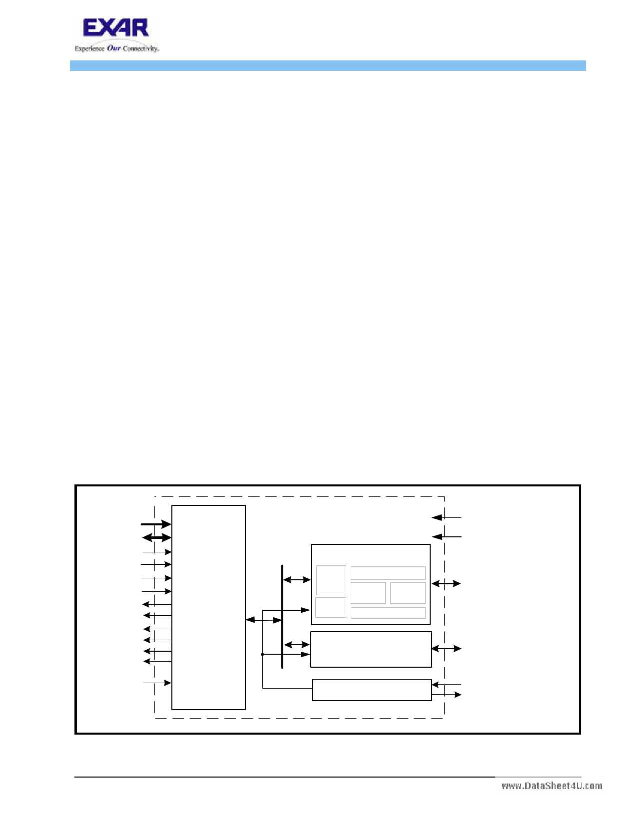
FIGURE 1. XR16M2550 BLOCK DIAGRAM
A2:A0
D7:D0
IOR#
IOW#
CSA#
CSB#
INTA
INTB
TXRDYA#
TXRDYB#
RXRDYA#
RXRDYB#
Reset
8-bit Data
Bus
Interface
UART Channel A
UART 16 Byte TX FIFO
Regs
TX & RX
IR
ENDEC
BRG 16 Byte RX FIFO
UART Channel B
(same as Channel A)
Crystal Osc/Buffer
1.62 to 3.63 Volt VCC
GND
TXA, RXA, DTRA#,
DSRA#, RTSA#,
DTSA#, CDA#, RIA#,
OP2A#
TXB, RXB, DTRB#,
DSRB#, RTSB#,
CTSB#, CDB#, RIB#,
OP2B#
XTAL1
XTAL2
Exar Corporation 48720 Kato Road, Fremont CA, 94538 • (510) 668-7000 • FAX (510) 668-7017 • www.exar.com
1 page 
www.DataSheet4U.com
REV. 1.0.1
Pin Description
XR16M2550
HIGH PERFORMANCE LOW VOLTAGE DUART WITH 16-BYTE FIFO
NAME
RTSB#
32-QFN
PIN #
15
48-TQFP
PIN #
22
CTSB#
16
23
DTRB#
DSRB#
-
-
35
20
CDB#
-
16
RIB#
-
21
OP2B#
-
9
ANCILLARY SIGNALS
XTAL1
10
XTAL2
11
RESET
24
13
14
36
VCC
GND
GND
26
13
Center Pad
42
17
N/A
NC 9, 17 12, 24, 25,
37
TYPE
DESCRIPTION
O UART channel B Request-to-Send (active low) or general purpose out-
put. This port must be asserted prior to using auto RTS flow control,
see EFR[6], MCR[1], and IER[6].
I UART channel B Clear-to-Send (active low) or general purpose input.
It can be used for auto CTS flow control, see EFR[7], and IER[7]. This
input should be connected to VCC when not used.
O UART channel B Data-Terminal-Ready (active low) or general purpose
output. If it is not used, leave it unconnected.
I UART channel B Data-Set-Ready (active low) or general purpose input.
This input should be connected to VCC when not used. This input has
no effect on the UART.
I UART channel B Carrier-Detect (active low) or general purpose input.
This input should be connected to VCC when not used. This input has
no effect on the UART.
I UART channel B Ring-Indicator (active low) or general purpose input.
This input should be connected to VCC when not used. This input has
no effect on the UART.
O Output Port 2 Channel B - The output state is defined by the user and
through the software setting of MCR[3]. INTB is set to the active mode
and OP2B# output LOW when MCR[3] is set to a logic 1. INTB is set to
the three state mode and OP2B# output HIGH when MCR[3] is set to a
logic 0. See MCR[3]. If INTB is used, this output should not be used as
a general output else it will disturb the INTB output functionality.
I Crystal or external clock input.
O Crystal or buffered clock output.
I Reset (active high) - A longer than 40 ns HIGH pulse on this pin will
reset the internal registers and all outputs. The UART transmitter output
will be held HIGH, the receiver input will be ignored and outputs are
reset during reset period (see Table 15).
Pwr 2.25V to 3.6V power supply.
Pwr Power supply common, ground.
Pwr The center pad on the backside of the 32-QFN package is metallic and
should be connected to GND on the PCB. The thermal pad size on the
PCB should be the approximate size of this center pad and should be
solder mask defined. The solder mask opening should be at least
0.0025" inwards from the edge of the PCB thermal pad.
No Connection.
Pin type: I=Input, O=Output, I/O= Input/output, OD=Output Open Drain.
5
5 Page 
www.DataSheet4U.com
REV. 1.0.1
XR16M2550
HIGH PERFORMANCE LOW VOLTAGE DUART WITH 16-BYTE FIFO
FIGURE 5. BAUD RATE GENERATOR
To Other
Channel
XTAL1
XTAL2
Crystal
Osc/
Buffer
Prescaler
Divide by 1
Prescaler
Divide by 4
DLL, DLM and DLD
Registers
MCR Bit-7=0
(default)
Fractional Baud
Rate Generator
Logic
16X or 8X or 4X
Sampling
Rate Clock
to Transmitter
and Receiver
MCR Bit-7=1
TABLE 5: TYPICAL DATA RATES WITH A 24 MHZ CRYSTAL OR EXTERNAL CLOCK AT 16X SAMPLING
Required
Output Data
Rate
400
2400
4800
9600
10000
19200
25000
28800
38400
50000
57600
75000
100000
115200
153600
200000
225000
230400
250000
300000
400000
460800
500000
750000
921600
1000000
DIVISOR FOR
16x Clock
(Decimal)
3750
625
312.5
156.25
150
78.125
60
52.0833
39.0625
30
26.0417
20
15
13.0208
9.7656
7.5
6.6667
6.5104
6
5
3.75
3.2552
3
2
1.6276
1.5
DIVISOR
OBTAINABLE IN
M2550
3750
625
312 8/16
156 4/16
150
78 2/16
60
52 1/16
39 1/16
30
26 1/16
20
15
13
9 12/16
7 8/16
6 11/16
6 8/16
6
5
3 12/16
3 4/16
3
2
1 10/16
1 8/16
DLM PROGRAM
VALUE (HEX)
E
2
1
0
0
0
0
0
0
0
0
0
0
0
0
0
0
0
0
0
0
0
0
0
0
0
DLL PROGRAM DLD PROGRAM
VALUE (HEX) VALUE (HEX)
A6 0
71 0
38 8
9C 4
96 0
4E 2
3C 0
34 1
27 1
1E 0
1A 1
14 0
F0
D0
9C
78
6B
68
60
50
3C
34
30
20
1A
18
DATA ERROR
RATE (%)
0
0
0
0
0
0
0
0.04
0
0
0.08
0
0
0.16
0.16
0
0.31
0.16
0
0
0
0.16
0
0
0.16
0
11
11 Page | ||
| Páginas | Total 47 Páginas | |
| PDF Descargar | [ Datasheet XR16M2550.PDF ] | |
Hoja de datos destacado
| Número de pieza | Descripción | Fabricantes |
| XR16M2550 | HIGH PERFORMANCE LOW VOLTAGE DUART | Exar Corporation |
| XR16M2551 | HIGH PERFORMANCE LOW VOLTAGE DUART | Exar Corporation |
| Número de pieza | Descripción | Fabricantes |
| SLA6805M | High Voltage 3 phase Motor Driver IC. |
Sanken |
| SDC1742 | 12- and 14-Bit Hybrid Synchro / Resolver-to-Digital Converters. |
Analog Devices |
|
DataSheet.es es una pagina web que funciona como un repositorio de manuales o hoja de datos de muchos de los productos más populares, |
| DataSheet.es | 2020 | Privacy Policy | Contacto | Buscar |