|
|
|
PDF AD5025 Data sheet ( Hoja de datos )
| Número de pieza | AD5025 | |
| Descripción | (AD5025 - AD5065) DAC SPI Interface | |
| Fabricantes | Analog Devices | |
| Logotipo | ||
Hay una vista previa y un enlace de descarga de AD5025 (archivo pdf) en la parte inferior de esta página. Total 28 Páginas | ||
|
No Preview Available !
Fully Accurate, 12-/14-/16-Bit, Dual, VOUT
nanoDAC SPI Interface, 4.5 V to 5.5 V in a TSSOP
AD5025/AD5045/AD5065
FEATURES
Low power dual 12-/14-/16-bit DAC, ±1 LSB INL
Individual voltage reference pins
Rail-to-rail operation
4.5 V to 5.5 V power supply
Power-on reset to zero scale or midscale
Power down to 400 nA @ 5 V
3 power-down functions
Per channel power-down
Low glitch upon power-up
Hardware power-down lockout capability
Hardware LDAC with software LDAC override function
CLR function to programmable code
SDO daisy-chaining option
14-lead TSSOP
APPLICATIONS
Process controls
Data acquisition systems
Portable battery-powered instruments
Digital gain and offset adjustment
Programmable voltage and current sources
Programmable attenuators
GENERAL DESCRIPTION
The AD5025/AD5045/AD5065 are low power, dual 12-/14-/16-bit
buffered voltage output nanoDAC® DACs offering relative accuracy
specifications of ±1 LSB INL with individual reference pins, and
can operate from a single 4.5 V to 5.5 V supply. The AD5025/
AD5045/AD5065 also offer a differential accuracy specification of
±1 LSB. The parts use a versatile 3-wire, low power Schmitt
trigger serial interface that operates at clock rates up to 50 MHz
and is compatible with standard SPI®, QSPI™, MICROWIRE™,
and DSP interface standards. The reference for the AD5025/
AD5045/AD5065 are supplied from an external pin and a refer-
ence buffer is provided on chip. The AD5025/AD5045/AD5065
incorporate a power-on reset circuit that ensures the DAC output
powers up zero scale or midscale and remains there until a valid
write takes place to the device. The AD5025/AD5045/AD5065
contain a power-down feature that reduces the current consump-
tion of the device to typically 400 nA at 5 V and provides software
selectable output loads while in power-down mode. The parts are
put into power-down mode over the serial interface. Total unad-
justed error for the parts is <2.5 mV. The parts exhibit very low
glitch on power-up. The outputs of all DACs can be updated
simultaneously using the LDAC function, with the added
functionality of user-selectable DAC channels to simultaneously
update. There is also an asynchronous CLR that clears all DACs
to a software-selectable code—0 V, midscale, or full scale. The
parts also feature a power-down lockout pin, PDL, which can be
used to prevent the DAC from entering power-down under any
circumstances over the serial interface.
PRODUCT HIGHLIGHTS
1. Dual channel available in a 14-lead TSSOP package with
individual voltage reference pins.
2. 12-/14-/16-bit accurate, ±1 LSB INL.
3. Low glitch on power-up.
4. High speed serial interface with clock speeds up to 50 MHz.
5. Three power-down modes available to the user.
6. Reset to known output voltage (zero scale or midscale).
7. Power-down lockout capability.
Table 1. Related Devices
Part No.
Description
AD5666
Quad,16-bit buffered DAC, 16 LSB INL, TSSOP
AD5024/AD5044/AD5064 Quad 16-bit nanoDAC, 1 LSB INL, TSSOP
AD5062/AD5063
16-bit nanoDAC, 1 LSB INL, MSOP
AD5061
16-bit nanoDAC, 4 LSB INL, SOT-23
AD5040/AD5060
14-/16-bit nanoDAC, 1 LSB INL, SOT-23
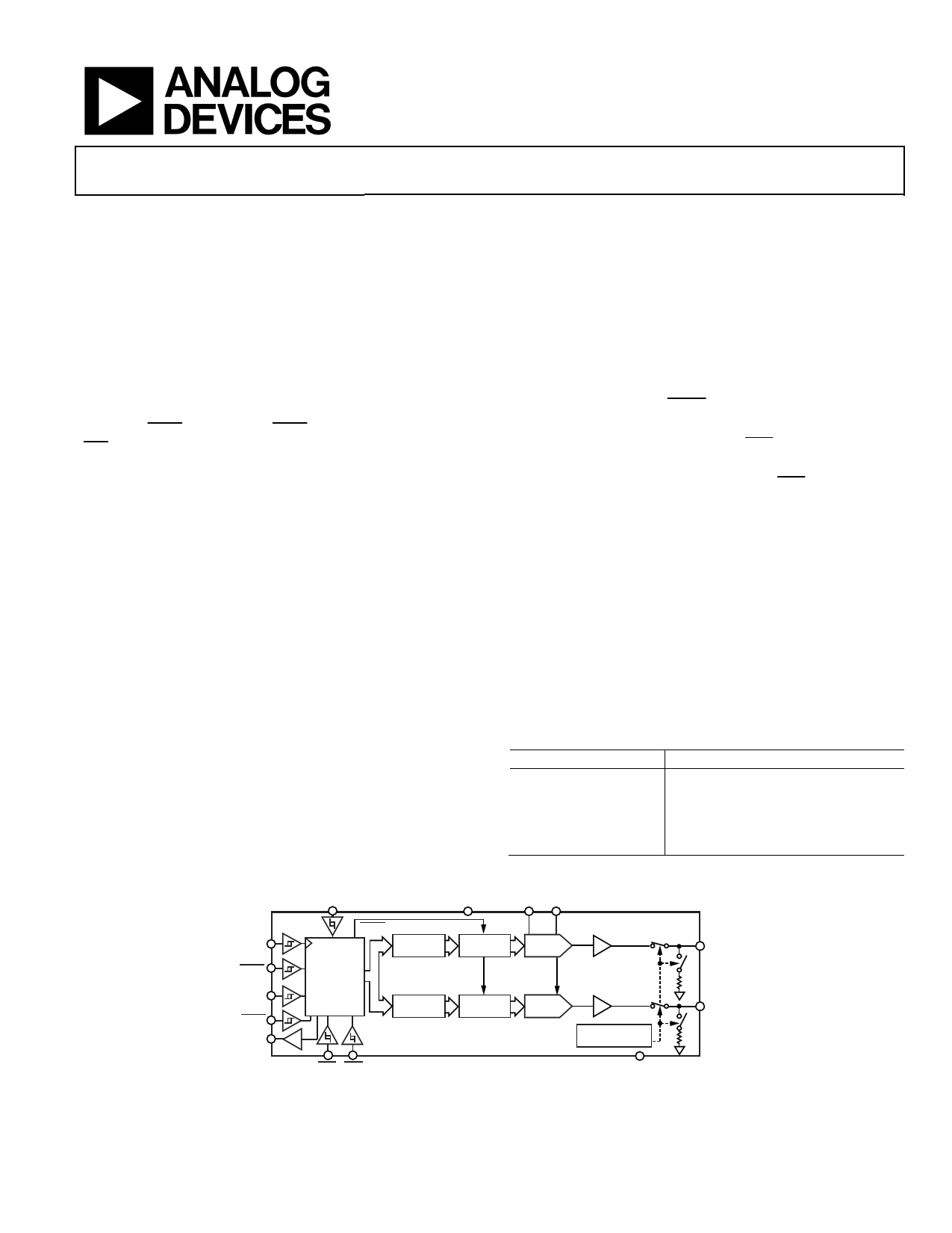
FUNCTIONAL BLOCK DIAGRAM
POR
VDD
VREFA VREFB
SCLK
SYNC
DIN
LDAC
SDO
LDAC
INPUT
REGISTER
INTERFACE
LOGIC
INPUT
REGISTER
DAC
REGISTER
DAC
REGISTER
DAC A
DAC B
PDL CLR
AD5025/AD5045/AD5065
Figure 1.
BUFFER
BUFFER
POWER-DOWN
LOGIC
GND
VOUTA
VOUTB
Rev. 0
Information furnished by Analog Devices is believed to be accurate and reliable. However, no
responsibility is assumed by Analog Devices for its use, nor for any infringements of patents or other
rights of third parties that may result from its use. Specifications subject to change without notice. No
license is granted by implication or otherwise under any patent or patent rights of Analog Devices.
Trademarksandregisteredtrademarksarethepropertyoftheirrespectiveowners.
One Technology Way, P.O. Box 9106, Norwood, MA 02062-9106, U.S.A.
Tel: 781.329.4700
www.analog.com
Fax: 781.461.3113
©2008 Analog Devices, Inc. All rights reserved.
1 page 
AD5025/AD5045/AD5065
TIMING CHARACTERISTICS
All input signals are specified with tR = tF = 1 ns/V (10% to 90% of VDD) and timed from a voltage level of (VIL + VIH)/2. See Figure 3 and
Figure 4. VDD = 4.5 V to 5.5 V. All specifications TMIN to TMAX, unless otherwise noted.
Table 4.
Parameter
SCLK Cycle Time
SCLK High Time
SCLK Low Time
SYNC to SCLK Falling Edge Setup Time
Data Setup Time
Data Hold Time
SCLK Falling Edge to SYNC Rising Edge
Minimum SYNC High Time (Single Channel Update)
Minimum SYNC High Time (All Channel Update)
SYNC Rising Edge to SCLK Fall Ignore
LDAC Pulse Width Low
SCLK Falling Edge to LDAC Rising Edge
CLR Pulse Width Low
SCLK Falling Edge to LDAC Falling Edge
CLR Pulse Activation Time
SCLK Rising Edge to SDO Valid
SCLK Falling Edge to SYNC Rising Edge
SYNC Rising Edge to SCLK Rising Edge
SYNC Rising Edge to LDAC/CLR/PDL Falling Edge (Single Channel Update)
SYNC Rising Edge to LDAC/CLR/PDL Falling Edge (All Channel Update)
PDL Minimum Pulse Width
Symbol
t11
t2
t3
t4
t5
t6
t7
t8
t8
t9
t10
t11
t12
t13
t14
t152, 3
t162
t172
t182
t182
t19
Min
20
10
10
16.5
5
5
0
2
4
17
20
20
10
10
10.6
5
8
2
4
20
Typ Max
30
22
30
Unit
ns
ns
ns
ns
ns
ns
ns
μs
μs
ns
ns
ns
ns
ns
μs
ns
ns
ns
μs
μs
ns
1 Maximum SCLK frequency is 50 MHz at VDD = 4.5 V to 5.5 V. Guaranteed by design and characterization; not production tested.
2 Daisy-chain mode only.
3 Measured with the load circuit of Figure 2. t15 determines the maximum SCLK frequency in daisy-chain mode.
Circuit and Timing Diagrams
2mA IOL
TO OUTPUT
PIN CL
50pF
VOH (MIN) + VOL (MAX)
2
2mA IOH
Figure 2. Load Circuit for Digital Output (SDO) Timing Specifications
Rev. 0 | Page 5 of 28
5 Page 
0.2
0.1
GAIN ERROR
0
FULL-SCALE ERROR
–0.1
–0.2
4.50
4.75 5.00 5.25
VDD (V)
5.50
Figure 18. Gain Error and Full-Scale Error vs. Supply Voltage
0.12
0.09
0.06
0.03
0
4.50
4.75
5.00
VDD (V)
5.25
Figure 19. Offset Error Voltage vs. Supply Voltage
5.50
16
14
12
10
8
6
4
2
0
0 1.0 1.1 1.2 1.3 1.4 1.5
IDD POWER UP (mA)
Figure 20. IDD Histogram, VDD = 5.0 V
AD5025/AD5045/AD5065
5.0
4.5
4.0
3.5
3.0 VDD = 5V, VREF = 4.096V
TA = 25ºC
2.5 1/4 SCALE TO 3/4 SCALE
3/4 SCALE TO 1/4 SCALE
2.0 OUTPUT LOADED WITH 5kΩ
AND 200pF TO GND
1.5
1.0
0.5
0
0 2 4 6 8 10 12 14
TIME (µs)
Figure 21. Settling Time and Typical Output Slew Rate
POR
1
VOUT
3
CH1 2V
CH3 2V
M2ms
T 20.4%
A CH1 2.52V
Figure 22. Power-On Reset to 0 V
1
3
CH1 2V
CH3 2V
M2ms
T 20.4%
A CH1 2.52V
Figure 23. Power-On Reset to Midscale
Rev. 0 | Page 11 of 28
11 Page | ||
| Páginas | Total 28 Páginas | |
| PDF Descargar | [ Datasheet AD5025.PDF ] | |
Hoja de datos destacado
| Número de pieza | Descripción | Fabricantes |
| AD502 | Operational Amplifier | Analog Devices |
| AD5024 | (AD50x4) DAC SPI Interface | Analog Devices |
| AD5025 | (AD5025 - AD5065) DAC SPI Interface | Analog Devices |
| AD5026 | 16-BIT CONSTANT-CURRENT LED DRIVER | AiT Semiconductor |
| Número de pieza | Descripción | Fabricantes |
| SLA6805M | High Voltage 3 phase Motor Driver IC. |
Sanken |
| SDC1742 | 12- and 14-Bit Hybrid Synchro / Resolver-to-Digital Converters. |
Analog Devices |
|
DataSheet.es es una pagina web que funciona como un repositorio de manuales o hoja de datos de muchos de los productos más populares, |
| DataSheet.es | 2020 | Privacy Policy | Contacto | Buscar |