|
|
|
PDF NTLJD3115P Data sheet ( Hoja de datos )
| Número de pieza | NTLJD3115P | |
| Descripción | Power MOSFET ( Transistor ) | |
| Fabricantes | ON Semiconductor | |
| Logotipo | ||
Hay una vista previa y un enlace de descarga de NTLJD3115P (archivo pdf) en la parte inferior de esta página. Total 7 Páginas | ||
|
No Preview Available !
NTLJD3115P
Power MOSFET
−20 V, −4.1 A, mCoolt Dual P−Channel,
2x2 mm WDFN Package
Features
• WDFN Package Provides Exposed Drain Pad for Excellent Thermal
Conduction
• 2x2 mm Footprint Same as SC−88
• Lowest RDS(on) Solution in 2x2 mm Package
• 1.8 V RDS(on) Rating for Operation at Low Voltage Gate Drive Logic
Level
• Low Profile (< 0.8 mm) for Easy Fit in Thin Environments
• Bidirectional Current Flow with Common Source Configuration
• This is a Pb−Free Device
Applications
• Optimized for Battery and Load Management Applications in
Portable Equipment
• Li−Ion Battery Charging and Protection Circuits
• High Side Load Switch
MAXIMUM RATINGS (TJ = 25°C unless otherwise noted)
www.DataSheet4U.com
Parameter
Symbol Value
Unit
Drain−to−Source Voltage
Gate−to−Source Voltage
Continuous Drain
Current (Note 1)
Steady
State
Power Dissipation
(Note 1)
t≤5s
Steady
State
Continuous Drain
Current (Note 2)
Power Dissipation
(Note 2)
t≤5s
Steady
State
TA = 25°C
TA = 85°C
TA = 25°C
TA = 25°C
TA = 25°C
TA = 85°C
TA = 25°C
VDSS
VGS
ID
PD
ID
PD
−20
±8.0
−3.3
−2.4
−4.1
1.5
2.3
−2.3
−1.6
0.71
V
V
A
W
A
W
Pulsed Drain Current
tp = 10 ms
IDM
Operating Junction and Storage Temperature TJ, TSTG
−20
−55 to
150
A
°C
Source Current (Body Diode) (Note 2)
Lead Temperature for Soldering Purposes
(1/8″ from case for 10 s)
IS −1.9 A
TL 260 °C
Maximum ratings are those values beyond which device damage can occur.
Maximum ratings applied to the device are individual stress limit values (not
normal operating conditions) and are not valid simultaneously. If these limits are
exceeded, device functional operation is not implied, damage may occur and
reliability may be affected.
1. Surface Mounted on FR4 Board using 1 in sq pad size (Cu area = 1.127 in sq
[2 oz] including traces).
2. Surface Mounted on FR4 Board using the minimum recommended pad size
of 30 mm2, 2 oz Cu.
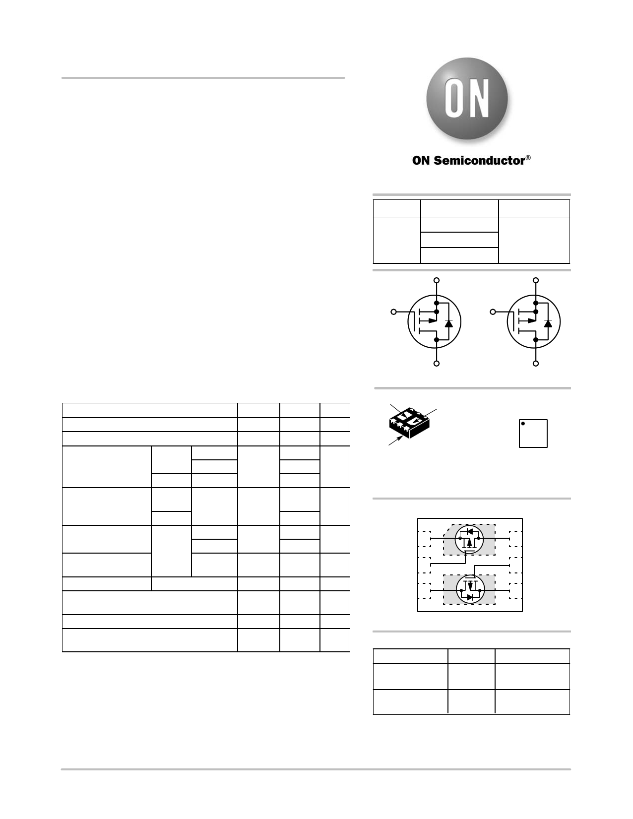
http://onsemi.com
V(BR)DSS
−20 V
RDS(on) MAX
100 mW @ −4.5 V
135 mW @ −2.5 V
200 mW @ −1.8 V
ID MAX (Note 1)
−4.1 A
S1 S2
G1 G2
D1 D2
P−CHANNEL MOSFET P−CHANNEL MOSFET
D2 D1
MARKING
DIAGRAM
Pin 1
WDFN6
CASE 506AN
1
2
JDMG
6
5
3G 4
JD = Specific Device Code
M = Date Code
G = Pb−Free Package
(Note: Microdot may be in either location)
PIN CONNECTIONS
S1 1
D1
6 D1
G1 2
D2 3
D2
5 G2
4 S2
(Top View)
ORDERING INFORMATION
Device
Package
Shipping†
NTLJD3115PT1G WDFN6 3000/Tape & Reel
(Pb−Free)
NTLJD3115PTAG WDFN6 3000/Tape & Reel
(Pb−Free)
†For information on tape and reel specifications,
including part orientation and tape sizes, please
refer to our Tape and Reel Packaging Specification
Brochure, BRD8011/D.
© Semiconductor Components Industries, LLC, 2006
June, 2006 − Rev. 4
1
Publication Order Number:
NTLJD3115P/D
1 page 
NTLJD3115P
TYPICAL PERFORMANCE CURVES (TJ = 25°C unless otherwise noted)
1200
VDS = 0 V VGS = 0 V
1000
Ciss
TJ = 25°C
5
4
QT
20
16
800
600
400 Crss
3 VDS
2 QGS
QGD
VGS 12
8
200 Coss
0
50
VGS
VDS
5
10 15
1
0
20 0
4
ID = −2.2 A
TJ = 25°C
0
12 3 456
QG, TOTAL GATE CHARGE (nC)
GATE−TO−SOURCE OR DRAIN−TO−SOURCE VOLTAGE (VOLTS)
Figure 7. Capacitance Variation
Figure 8. Gate−To−Source and Drain−To−Source
Voltage versus Total Charge
1000
VDD = −15 V
ID = −2.2 A
VGS = −4.5 V
100
tf
tr
10 td(off)
td(on)
1
1 10 100
RG, GATE RESISTANCE (OHMS)
Figure 9. Resistive Switching Time
Variation versus Gate Resistance
3
VGS = 0 V
2.5
2
1.5
1
0.5
TJ = 150°C
TJ = 25°C
0
0 0.1 0.2 0.3 0.4 0.5 0.6 0.7 0.8 0.9 1.0
−VSD, SOURCE−TO−DRAIN VOLTAGE (VOLTS)
Figure 10. Diode Forward Voltage versus Current
100
TC = 25°C
TJ = 150°C
SINGLE PULSE
10
1
10 ms
100 ms
1 ms
10 ms
*See Note 2 on Page 1
0.1
RDS(on) LIMIT
THERMAL LIMIT
0.01
0.1
PACKAGE LIMIT
1
dc
10
100
−VDS, DRAIN−TO−SOURCE VOLTAGE (VOLTS)
Figure 11. Maximum Rated Forward Biased
Safe Operating Area
http://onsemi.com
5
5 Page | ||
| Páginas | Total 7 Páginas | |
| PDF Descargar | [ Datasheet NTLJD3115P.PDF ] | |
Hoja de datos destacado
| Número de pieza | Descripción | Fabricantes |
| NTLJD3115P | Power MOSFET ( Transistor ) | ON Semiconductor |
| Número de pieza | Descripción | Fabricantes |
| SLA6805M | High Voltage 3 phase Motor Driver IC. |
Sanken |
| SDC1742 | 12- and 14-Bit Hybrid Synchro / Resolver-to-Digital Converters. |
Analog Devices |
|
DataSheet.es es una pagina web que funciona como un repositorio de manuales o hoja de datos de muchos de los productos más populares, |
| DataSheet.es | 2020 | Privacy Policy | Contacto | Buscar |