|
|
|
PDF ADATE207 Data sheet ( Hoja de datos )
| Número de pieza | ADATE207 | |
| Descripción | Quad Pin Timing Formatter | |
| Fabricantes | Analog Devices | |
| Logotipo | ||
Hay una vista previa y un enlace de descarga de ADATE207 (archivo pdf) en la parte inferior de esta página. Total 36 Páginas | ||
|
No Preview Available !
FEATURES
4-channel timing formatter
256 waveforms per channel
4 independent event edges per waveform
STIL IEEE 1450-1999-compatible events
4-period range for each edge
39.06 ps timing resolution
2.5 ns minimum edge refire rate
All drive formats supported
100 MHz base vector rate
×2 and ×4 high speed modes
×2 pin multiplexing
1 ns minimum pulse width
32-bit fail counter per channel
4-bit pin capture per channel
Air cooled, low power CMOS design
6 W at 100 MHz base rate
2.5 V power supply
Differential DCL interface control
TMU multiplexer
www.DataSheet4U.com
APPLICATIONS
Automatic test equipment (ATE)
High speed digital instrumentation
Pulse generation
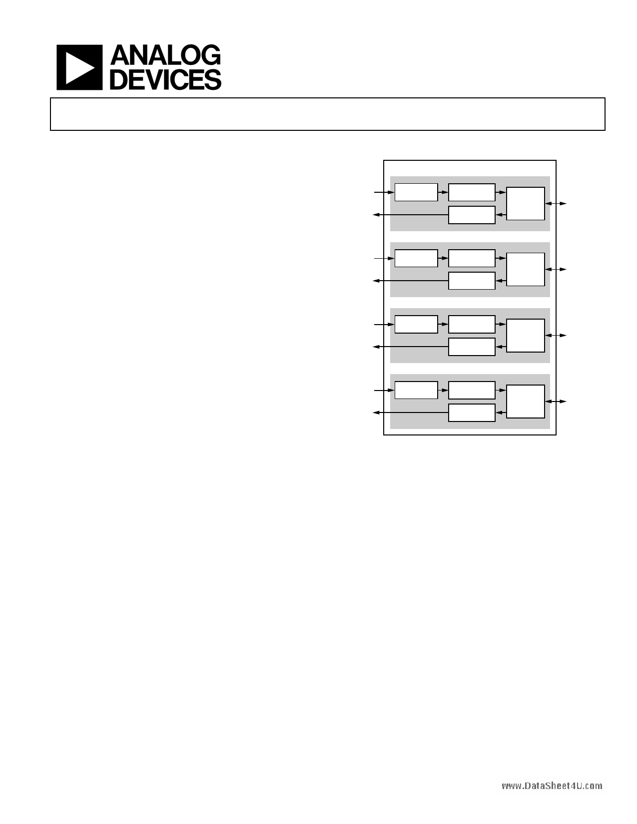
GENERAL DESCRIPTION
The ADATE207 is a timing generator and formatter for auto-
matic test equipment (ATE) equipment. The ADATE207 provides
four independent channels with a 100 MHz base vector rate of
timing and formatting for ATE digital pins. It interfaces between
the pattern memory,and the driver, comparator, and load (DCL)
chips for complete digital pins. The ADATE207 accepts up to
eight bits of pattern data per pin and can produce formatted
outputs and perform comparisons of DUT expected responses.
Each channel of the ADATE207 provides 256 selectable wave-
forms, wherein each waveform consists of up to four possible
events. Each event consists of a programmable timing edge and a
STIL-compatible (IEEE Standard 1450-1999) set.
Each timing edge generator can produce an edge with a span of
four periods with a 39.06 ps edge placement resolution. The delay
Quad Pin Timing Formatter
ADATE207
FUNCTIONAL BLOCK DIAGRAM
ADATE207
PATTERN
FAIL
TIME SET
MEMORY
QUAD EDGE
GENERATOR
FAIL
DETECTION
FORMAT
COMPARE
LOGIC
DCL
INTERFACE
PATTERN
FAIL
TIME SET
MEMORY
QUAD EDGE
GENERATOR
FAIL
DETECTION
FORMAT
COMPARE
LOGIC
DCL
INTERFACE
PATTERN
FAIL
TIME SET
MEMORY
QUAD EDGE
GENERATOR
FAIL
DETECTION
FORMAT
COMPARE
LOGIC
DCL
INTERFACE
PATTERN
FAIL
TIME SET
MEMORY
QUAD EDGE
GENERATOR
FAIL
DETECTION
FORMAT
COMPARE
LOGIC
DCL
INTERFACE
Figure 1.
generators use a reference master clock of 100 MHz and provide
programmable delays based upon counts of the clock and a
compensated CMOS analog timing vernier. The programmable
delay generators can be additionally delayed by a global 8-bit
input value that is shared across all edges.
The format and compare logic support ×2 pin multiplexing to
allow the trading of pin count for speed.
Each channel provides a 4-bit DUT output capture supporting
mixed signal receive memory applications. The fail detection
logic includes a 32-bit fail accumulation register per channel.
An external TMU is supported with three 8-to-1 multiplexers.
This allows the dual comparator outputs of any pin to be
multiplexed to any of the three outputs: arm, start, or stop
signals.
Rev. 0
Information furnished by Analog Devices is believed to be accurate and reliable. However, no
responsibility is assumed by Analog Devices for its use, nor for any infringements of patents or other
rights of third parties that may result from its use. Specifications subject to change without notice. No
license is granted by implication or otherwise under any patent or patent rights of Analog Devices.
Trademarksandregisteredtrademarksarethepropertyoftheirrespectiveowners.
One Technology Way, P.O. Box 9106, Norwood, MA 02062-9106, U.S.A.
Tel: 781.329.4700
www.analog.com
Fax: 781.461.3113
©2007 Analog Devices, Inc. All rights reserved.
1 page 
TIMING DIAGRAMS
MCLK_P
MCLK_N
DIGITAL INPUTS
tISU tIH
DIGITAL OUTPUTS
JTAG
JTAG INPUT
tOCO(MIN)
tOCO(MAX)
Figure 2. Timing Diagram for Inputs and Outputs
tJSU
tJH
www.DataSheet4U.com
JTAG OUTPUT
MCLK_P
MCLK_N
BIDIRECTIONAL (WRITES)
tJCO
Figure 3. Timing Diagram for Scan Inputs and Scan Outputs
tBSU
tBH
tBCZV
BIDIRECTIONAL (READS)
tBCO(MIN)
tBCO(MAX)
tBCZ
Figure 4. Timing Diagram for Bidirectional Reads and Writes
ADATE207
Rev. 0 | Page 5 of 36
5 Page 
Pin No.
Y20 to Y18, Y12, Y11, Y8, Y3 to
Y1, W20, W1, V20, V1, N20, N1,
K20, K1, J20, J1, C20, C1, B20,
B1, A20 to A18, A13, A10, A9
W19, W18, W3, W2, V19, V18,
V3, V2, U17, U14, U11, U7, U4,
P17, P4, K17, K4, G17, G4,
D17, D14, D10, D7, D4, C19,
C18, C3, C2, B19, B18, B3, B2
Mnemonic
VSS
VDD
1 A = analog, D = differential, I = input, O = output, P = power.
Input/Output1 Type
P GND
P VDD
Description
Power, 0.0 V.
Power, 2.5 V.
ADATE207
www.DataSheet4U.com
Rev. 0 | Page 11 of 36
11 Page | ||
| Páginas | Total 36 Páginas | |
| PDF Descargar | [ Datasheet ADATE207.PDF ] | |
Hoja de datos destacado
| Número de pieza | Descripción | Fabricantes |
| ADATE205 | Dual DCL | Analog Devices |
| ADATE206 | Dual DCL | Analog Devices |
| ADATE207 | Quad Pin Timing Formatter | Analog Devices |
| ADATE209 | 4.0 Gbps Dual Driver | Analog Devices |
| Número de pieza | Descripción | Fabricantes |
| SLA6805M | High Voltage 3 phase Motor Driver IC. |
Sanken |
| SDC1742 | 12- and 14-Bit Hybrid Synchro / Resolver-to-Digital Converters. |
Analog Devices |
|
DataSheet.es es una pagina web que funciona como un repositorio de manuales o hoja de datos de muchos de los productos más populares, |
| DataSheet.es | 2020 | Privacy Policy | Contacto | Buscar |