|
|
|
PDF AD9912 Data sheet ( Hoja de datos )
| Número de pieza | AD9912 | |
| Descripción | 1 GSPS Direct Digital Synthesizer | |
| Fabricantes | Analog Devices | |
| Logotipo | ||
Hay una vista previa y un enlace de descarga de AD9912 (archivo pdf) en la parte inferior de esta página. Total 30 Páginas | ||
|
No Preview Available !
FEATURES
1 GSPS internal clock speed (up to 400 MHz output directly)
Integrated 1 GSPS 14-bit DAC
48-bit frequency tuning word with 4 μHz resolution
Differential HSTL comparator
Flexible system clock input accepts either crystal or external
reference clock
On-chip low noise PLL REFCLK multiplier
2 SpurKiller channels
Low jitter clock doubler for frequencies up to 750 MHz
Single-ended CMOS comparator; frequencies of <150 MHz
Programmable output divider for CMOS output
Serial I/O control
Excellent dynamic performance
Software controlled power-down
Available in two 64-lead LFCSP packages
Residual phase noise @ 250 MHz
10 Hz offset: −113 dBc/Hz
1 kHz offset: −133 dBc/Hz
100 kHz offset: −153 dBc/Hz
40 MHz offset: −161 dBc/Hz
1 GSPS Direct Digital
Synthesizer with 14-Bit DAC
AD9912
APPLICATIONS
Agile LO frequency synthesis
Low jitter, fine tune clock generation
Test and measurement equipment
Wireless base stations and controllers
Secure communications
Fast frequency hopping
GENERAL DESCRIPTION
The AD9912 is a direct digital synthesizer (DDS) that features
an integrated 14-bit digital-to-analog converter (DAC). The
AD9912 features a 48-bit frequency tuning word (FTW) that
can synthesize frequencies in step sizes no larger than 4 μHz.
Absolute frequency accuracy can be achieved by adjusting the
DAC system clock.
The AD9912 also features an integrated system clock phase-
locked loop (PLL) that allows for system clock inputs as low
as 25 MHz.
The AD9912 operates over an industrial temperature range,
spanning −40°C to +85°C.
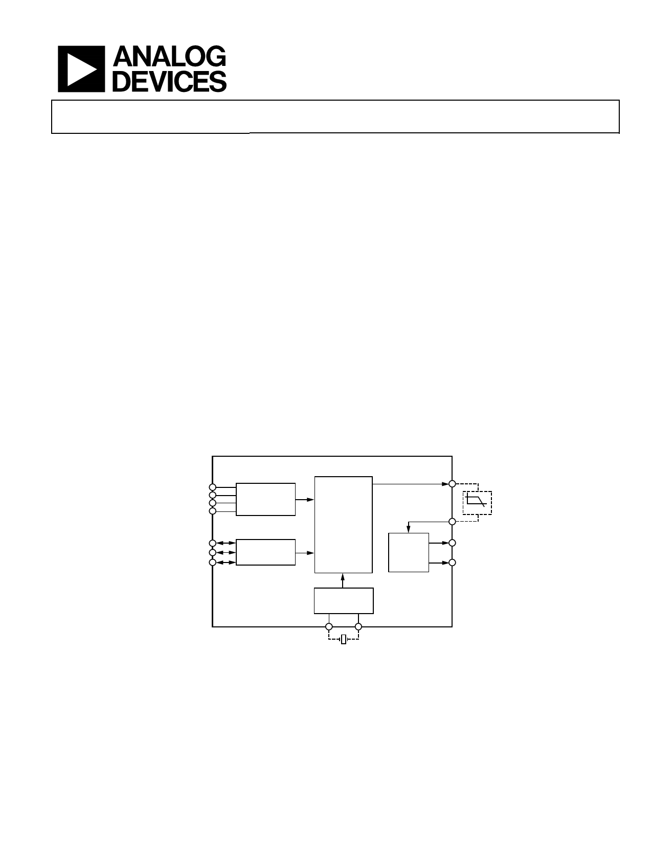
S1 TO S4
DIGITAL
INTERFACE
BASIC BLOCK DIAGRAM
AD9912
STARTUP
CONFIGURATION
LOGIC
SERIAL PORT,
I/O LOGIC
DIRECT
DIGITAL
SYNTHESIS
CORE
DAC_OUT
FDBK_IN
FILTER
CLOCK
OUTPUT
DRIVERS
OUT
OUT_CMOS
SYSTEM CLOCK
MULTIPLIER
Figure 1.
Rev. F
Information furnished by Analog Devices is believed to be accurate and reliable. However, no
responsibility is assumed by Analog Devices for its use, nor for any infringements of patents or other
rights of third parties that may result from its use. Specifications subject to change without notice. No
license is granted by implication or otherwise under any patent or patent rights of Analog Devices.
Trademarksandregisteredtrademarksarethepropertyoftheirrespectiveowners.
One Technology Way, P.O. Box 9106, Norwood, MA 02062-9106, U.S.A.
Tel: 781.329.4700
www.analog.com
Fax: 781.461.3113 ©2007–2010 Analog Devices, Inc. All rights reserved.
1 page 
REVISION HISTORY
6/10—Rev. E to Rev. F
Changed Default Value of Register 0x003 to 0x19 (Table 12).....31
5/10—Rev. D to Rev. E
Deleted 64-Lead LFCSP (CP-64-1).................................. Universal
Changes to SYSCLK PLL Enabled/ Maximum Input Rate of System
Clock PFD, Table 2 ...............................................................................6
Updated Outline Dimensions........................................................39
Changes to Ordering Guide...........................................................39
11/09—Rev. C to Rev. D
Added 64-Lead LFCSP (CP-64-7).................................... Universal
Changes to Serial Port Timing Specifications and
Propagation Delay Parameters ........................................................6
Added Exposed Paddle Notation to Figure 2 ................................8
Changes to Power Supply Partitioning Section...........................25
Change to Serial Control Port Section .........................................26
Changes to Figure 52 ......................................................................28
Added Exposed Paddle Notation to Outline Dimensions.........38
Changes to Ordering Guide...........................................................39
AD9912
7/09—Rev. B to Rev. C
Changes to Logic Outputs Parameter, Table 1 ..............................3
Changes to AVDD (Pin 25, Pin 26, Pin 29, and Pin 30) ............25
6/09—Rev. A to Rev. B
Changes to Figure 40 and Direct Digital Synthesizer Section ..17
Changes to Figure 48 ......................................................................22
Changes to Table 11 ........................................................................30
Changes to Table 22 and Table 23.................................................34
1/08—Rev. 0 to Rev. A
Changes to Table 1 ............................................................................3
Changes to Table 2 ............................................................................5
Changes to Table 4 ............................................................................8
Changes to Typical Performance Characteristics .......................10
Changes to Functional Description Section................................19
Changes to Single-Ended CMOS Output Section ......................21
Changes to Harmonic Spur Reduction Section ..........................21
Changes to Power Supply Partitioning Section...........................25
10/07—Revision 0: Initial Version
Rev. F | Page 3 of 40
5 Page 
PIN CONFIGURATION AND FUNCTION DESCRIPTIONS
AD9912
DVDD_I/O 1
DVSS 2
DVDD 3
DVSS 4
DVDD 5
DVSS 6
DVDD 7
DVSS 8
S1 9
S2 10
AVDD 11
NC 12
NC 13
AVDD3 14
NC 15
NC 16
PIN 1
INDICATOR
AD9912
TOP VIEW
(Not to Scale)
48 DAC_RSET
47 AVDD3
46 AVDD3
45 AVDD
44 AVDD
43 AVSS
42 AVDD
41 FDBK_IN
40 FDBK_INB
39 AVSS
38 OUT_CMOS
37 AVDD3
36 AVDD
35 OUT
34 OUTB
33 AVSS
NOTES
1. NC = NO CONNECT.
2. THE EXPOSED PAD MUST BE CONNECTED TO GROUND FOR PROPER OPERATION.
Figure 2. Pin Configuration
Table 5. Pin Function Descriptions
Pin No.
Input/
Output Pin Type
1 I Power
2, 4, 6, 8
I Power
3, 5, 7
I Power
9, 10, 54, 55 I/O 3.3 V CMOS
11, 19, 23 to 26,
29, 30, 36, 42, 44,
45, 53
12, 13, 15, 16, 17,
18, 20, 21, 22
14, 46, 47, 49
27
I
I
I
Power
Power
Differential
input
28 I Differential
input
31 O
Mnemonic
DVDD_I/O
DVSS
DVDD
S1, S2, S3, S4
AVDD
NC
AVDD3
SYSCLK
SYSCLKB
LOOP_FILTER
Description
I/O Digital Supply.
Digital Ground. Connect to ground.
Digital Supply.
Start-Up Configuration Pins. These pins are configured under program
control and do not have internal pull-up/pull-down resistors.
Analog Supply. Connect to a nominal 1.8 V supply.
No Connect. These unused pins can be left unconnected.
Analog Supply. Connect to a nominal 3.3 V supply.
System Clock Input. The system clock input has internal dc biasing and
should always be ac-coupled, except when using a crystal. Single-ended
1.8 V CMOS can also be used, but it may introduce a spur caused by an input
duty cycle that is not 50%. When using a crystal, tie the CLKMODESEL pin
to AVSS, and connect crystal directly to this pin and Pin 28.
Complementary System Clock. Complementary signal to the input
provided on Pin 27. Use a 0.01 μF capacitor to ground on this pin if the
signal provided on Pin 27 is single-ended.
System Clock Multiplier Loop Filter. When using the frequency multiplier to
drive the system clock, an external loop filter must be constructed and
attached to this pin. This pin should be pulled down to ground with 1 kΩ
resistor when the system clock PLL is bypassed. See Figure 46 for a diagram
of the system clock PLL loop filter.
Rev. F | Page 9 of 40
11 Page | ||
| Páginas | Total 30 Páginas | |
| PDF Descargar | [ Datasheet AD9912.PDF ] | |
Hoja de datos destacado
| Número de pieza | Descripción | Fabricantes |
| AD9910 | 3.3V CMOS Direct Digital Synthesizer | Analog Devices |
| AD9911 | 500 MSPS Direct Digital Synthesizer | Analog Devices |
| AD9912 | 1 GSPS Direct Digital Synthesizer | Analog Devices |
| AD9913 | Low Power 250 MSPS 10-Bit DAC 1.8V CMOS Direct Digital Synthesizer | Analog Devices |
| Número de pieza | Descripción | Fabricantes |
| SLA6805M | High Voltage 3 phase Motor Driver IC. |
Sanken |
| SDC1742 | 12- and 14-Bit Hybrid Synchro / Resolver-to-Digital Converters. |
Analog Devices |
|
DataSheet.es es una pagina web que funciona como un repositorio de manuales o hoja de datos de muchos de los productos más populares, |
| DataSheet.es | 2020 | Privacy Policy | Contacto | Buscar |