|
|
|
PDF DG200A Data sheet ( Hoja de datos )
| Número de pieza | DG200A | |
| Descripción | Monolithic Dual SPST CMOS Analog Switch | |
| Fabricantes | Vishay Siliconix | |
| Logotipo | ||
Hay una vista previa y un enlace de descarga de DG200A (archivo pdf) en la parte inferior de esta página. Total 5 Páginas | ||
|
No Preview Available !
DG200A_MIL
Vishay Siliconix
Monolithic Dual SPST CMOS Analog Switch
FEATURES
D "15 V Input Signal Range
D 44-V Maximum Supply Ranges
D On-Resistance: 45 W
D TTL and CMOS Compatibility
BENEFITS
D Wide Dynamic Range
D Simple Interfacing
D Reduced External Component
Count
APPLICATIONS
D Servo Control Switching
D Programmable Gain Amplifiers
D Audio Switching
D Programmable Filters
DESCRIPTION
The DG200A_MIL is a dual, single-pole, single-throw analog
switch designed to provide general purpose switching of
analog signals. This device is ideally suited for designs
requiring a wide analog voltage range coupled with low
on-resistance.
The DG200A_MIL is designed on Vishay Siliconix’ improved
PLUS-40 CMOS process. An epitaxial layer prevents latchup.
Each switch conducts equally well in both directions when on,
and blocks up to 30 V peak-to-peak when off. In the on
condition, this bi-directional switch introduces no offset
voltage of its own.
www.DataSheet4U.com
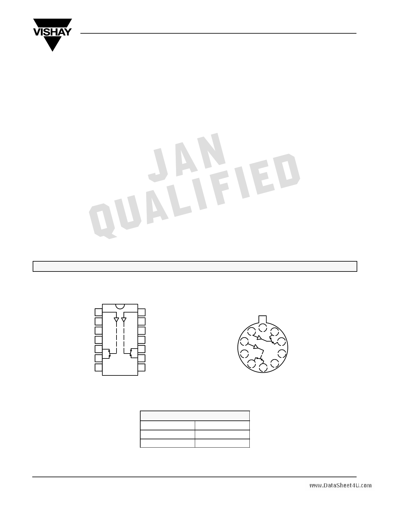
FUNCTIONAL BLOCK DIAGRAM AND PIN CONFIGURATION
Dual-In-Line
IN2
NC
GND
NC
S2
D2
V–
1
2
3
4
5
6
7
14 IN1
13 NC
12 V+ Substrate
11 NC
10 S1
9 D1
8 NC
Top View
Metal Can
V+ (Substrate and Case)
IN1 10 S1
19
IN2
2
D1
8
GND 3
7 NC
46
S2 5 V–
D2
Top View
Document Number: 70035
S-02314—Rev. E, 05-Oct-00
TRUTH TABLE
Logic
Switch
0 ON
1 OFF
Logic “0” v 0.8 V
Logic “1” w 2.4 V
www.vishay.com
4-1
1 page 
DG200A_MIL
Vishay Siliconix
TEST CIRCUITS
VO is the steady state output with switch on. Feedthrough via gate capacitance may result in spikes at leading and trailing edge of output waveform.
+15 V
Logic
Input
3V
0V
Switch
Input
VS
Switch
Output
VO
50%
90%
tr <20 ns
tf <20 ns
tOFF
VS = +5 V
3V
V+
SD
IN
GND
V–
RL
1 kW
VO
CL
35 pF
tON –15 V
RL
FIGURE 2. Switching Time
VO = VS
RL + rDS(on)
+15 V
V+
Rg S
D
VO
DVO
VO
www.DataSheet4U.com
Vg
3V
IN
GND
V–
CL
1000 pF
INX ON
OFF
ON
–15 V
DVO = measured voltage error due to charge injection
The charge injection in coulombs is DQ = CL x DVO
FIGURE 3. Charge Injection
VS
Rg = 50 W
5V
+15 V
C
V+
SD
IN
GND
V– C
VO
RL
–15 V
Off Isolation = 20 log
VS
VO
FIGURE 4. Off Isolation
Document Number: 70035
S-02314—Rev. E, 05-Oct-00
+15 V
C
VS
Rg = 50 W
0V
NC
0V
V+
S1 D1
IN1
S2 D2
IN2
GND
V– C
50 W
VO
RL
–15 V
XTALK = 20 log
C = RF bypass
VS
VO
FIGURE 5. Channel-to-Channel Crosstalk
www.vishay.com
4-5
5 Page | ||
| Páginas | Total 5 Páginas | |
| PDF Descargar | [ Datasheet DG200A.PDF ] | |
Hoja de datos destacado
| Número de pieza | Descripción | Fabricantes |
| DG200 | Dual Monolithic SPST CMOS Analog Switch | Maxim Integrated |
| DG200 | Monolithic Dual SPST CMOS Analog Switch | TEMICs |
| DG200 | CMOS Dual/Quad SPST Analog Switches | Harris Corporation |
| DG2001 | LOW - VOLTAGE SINGLE SPDT ANALOG SWITCH | Vishay Siliconix |
| Número de pieza | Descripción | Fabricantes |
| SLA6805M | High Voltage 3 phase Motor Driver IC. |
Sanken |
| SDC1742 | 12- and 14-Bit Hybrid Synchro / Resolver-to-Digital Converters. |
Analog Devices |
|
DataSheet.es es una pagina web que funciona como un repositorio de manuales o hoja de datos de muchos de los productos más populares, |
| DataSheet.es | 2020 | Privacy Policy | Contacto | Buscar |