|
|
|
PDF FDD6635 Data sheet ( Hoja de datos )
| Número de pieza | FDD6635 | |
| Descripción | 35V N-Channel PowerTrench MOSFET | |
| Fabricantes | Fairchild Semiconductor | |
| Logotipo | ||
Hay una vista previa y un enlace de descarga de FDD6635 (archivo pdf) en la parte inferior de esta página. Total 8 Páginas | ||
|
No Preview Available !
www.DataSheet4U.com
February 2007
FDD6635
35V N-Channel PowerTrench® MOSFET
tm
General Description
This N-Channel MOSFET has been produced using
Fairchild Semiconductor’s proprietary PowerTrench
technology to deliver low Rdson and optimized Bvdss
capability to offer superior performance benefit in the
applications.
Applications
• Inverter
• Power Supplies
Features
• 59 A, 35 V
RDS(ON) = 10 mΩ @ VGS = 10 V
RDS(ON) = 13 mΩ @ VGS = 4.5 V
• Fast Switching
• RoHS compliant
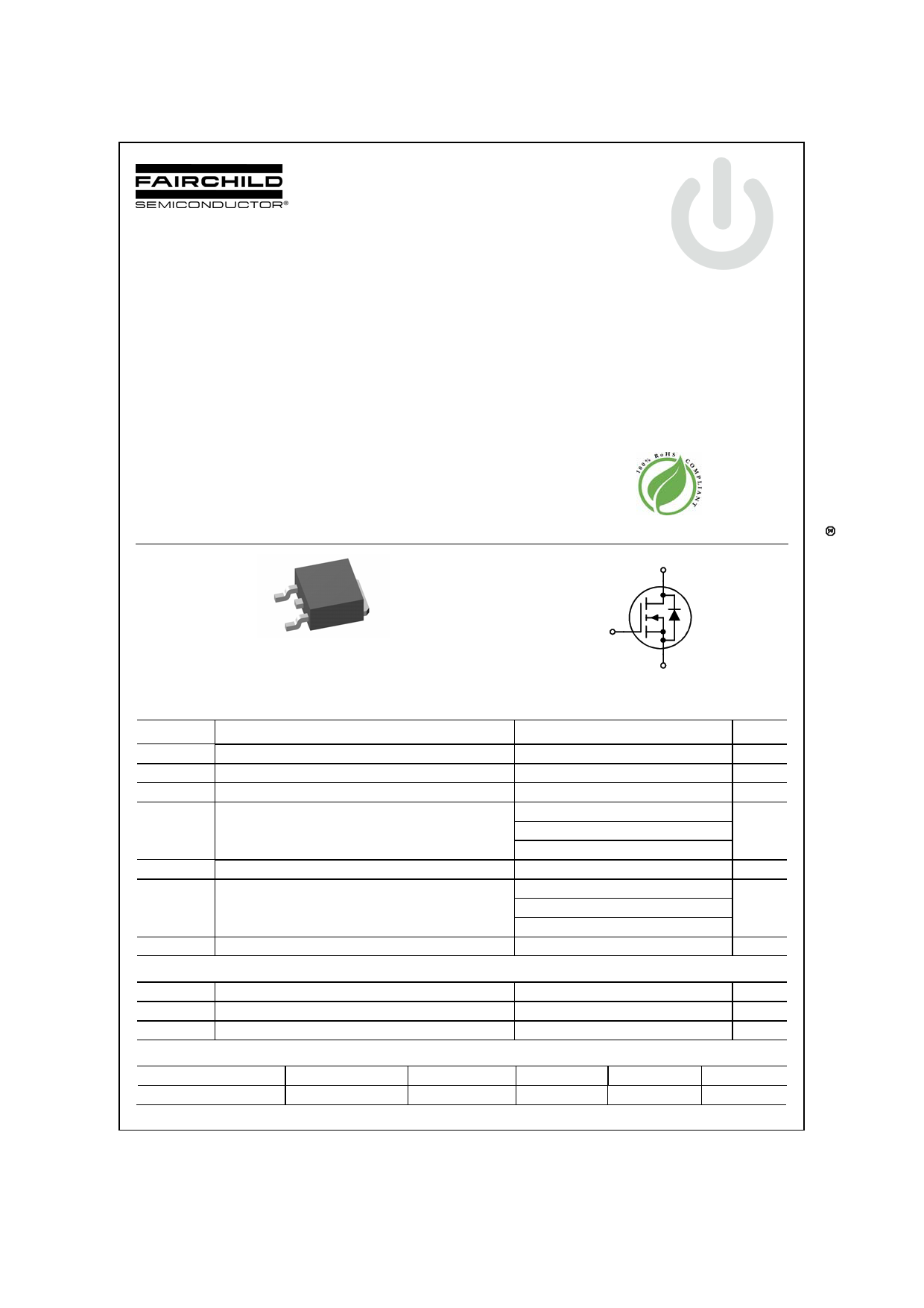
D
G
S
DTO-P-2A5K2
(TO-252)
D
G
S
Absolute Maximum Ratings TA=25oC unless otherwise noted
Symbol
VDSS
VDS(Avalanche)
VGSS
ID
Parameter
Drain-Source Voltage
Drain-Source Avalanche Voltage (maximum) (Note 4)
Gate-Source Voltage
Continuous Drain Current @TC=25°C
(Note 3)
@TA=25°C
(Note 1a)
Pulsed
(Note 1a)
Ratings
35
40
±20
59
15
100
EAS
PD
TJ, TSTG
Single Pulse Avalanche Energy
(Note 5)
Power Dissipation
@TC=25°C
(Note 3)
@TA=25°C
(Note 1a)
@TA=25°C
(Note 1b)
Operating and Storage Junction Temperature Range
113
55
3.8
1.6
–55 to +150
Thermal Characteristics
RθJC
Thermal Resistance, Junction-to-Case
(Note 1)
RθJA Thermal Resistance, Junction-to-Ambient (Note 1a)
RθJA Thermal Resistance, Junction-to-Ambient (Note 1b)
2.7
40
96
Package Marking and Ordering Information
Device Marking
Device
Package
Reel Size
Tape width
FDD6635
FDD6635
D-PAK (TO-252)
13’’
12mm
Units
V
V
V
A
mJ
W
°C
°C/W
°C/W
°C/W
Quantity
2500 units
©2007 Fairchild Semiconductor Corporation
FDD6635 Rev. C2(W)
www.fairchildsemi.com
1 page 
Typical Characteristics
10
ID = 15A
8
6
VDS = 10V
20V
15V
4
2
0
0 5 10 15 20 25 30
Qg, GATE CHARGE (nC)
Figure 7. Gate Charge Characteristics
1000
RDS(ON) LIMIT
100
10
1
VGS = 10V
SINGLE PULSE
0.1 RθJA = 96oC/W
TA = 25oC
100µs
10s
DC
1ms
10ms
100ms
1s
0.01
0.01
0.1 1 10
VDS, DRAIN-SOURCE VOLTAGE (V)
100
Figure 9. Maximum Safe Operating Area
100
SINGLE PULSE
RθJA = 96癈 /W
80 TA = 25癈
60
40
20
0
0.1
1 10 100
t1, TIME (sec)
1000
Figure 11. Single Pulse Maximum Peak
Current
2000
f = 1MHz
VGS = 0 V
1600
CISS
1200
800
400
0
0
COSS
CRSS
5 10 15 20 25
VDS, DRAIN TO SOURCE VOLTAGE (V)
30
Figure 8. Capacitance Characteristics
100
SINGLE PULSE
80 RθJA = 96°C/W
TA = 25°C
60
40
20
0
0.01
0.1
1 10
t1, TIME (sec)
100
Figure 10. Single Pulse Maximum
Power Dissipation
1000
1000
TJ = 25oC
100
10
1
0.001
0.01
0.1
1
tAV, TIME IN AVANCHE(ms)
10
Figure 12. Unclamped Inductive Switching
Capability
FDD6635 Rev. C2(W)
www.fairchildsemi.com
5 Page | ||
| Páginas | Total 8 Páginas | |
| PDF Descargar | [ Datasheet FDD6635.PDF ] | |
Hoja de datos destacado
| Número de pieza | Descripción | Fabricantes |
| FDD6630A | N-Channel PowerTrench MOSFET | Fairchild Semiconductor |
| FDD6632 | N-Channel Logic Level UltraFET Trench Power MOSFET 30V/ 9A/ 90m | Fairchild Semiconductor |
| FDD6635 | 35V N-Channel PowerTrench MOSFET | Fairchild Semiconductor |
| FDD6637 | 35V P-Channel PowerTrench MOSFET | Fairchild Semiconductor |
| Número de pieza | Descripción | Fabricantes |
| SLA6805M | High Voltage 3 phase Motor Driver IC. |
Sanken |
| SDC1742 | 12- and 14-Bit Hybrid Synchro / Resolver-to-Digital Converters. |
Analog Devices |
|
DataSheet.es es una pagina web que funciona como un repositorio de manuales o hoja de datos de muchos de los productos más populares, |
| DataSheet.es | 2020 | Privacy Policy | Contacto | Buscar |