|
|
|
PDF XC9508 Data sheet ( Hoja de datos )
| Número de pieza | XC9508 | |
| Descripción | Synchronous Step-Down DC/DC Converter | |
| Fabricantes | Torex Semiconductor | |
| Logotipo | ||
Hay una vista previa y un enlace de descarga de XC9508 (archivo pdf) en la parte inferior de esta página. Total 30 Páginas | ||
|
No Preview Available !
June 9, 2005 V7
◆Synchronous Step-Down DC/DC Converter with
Built-In LDO Regulator plus Voltage Detector
◆Step-Down DC/DC Converter's Output Connected in
Series with LDO Regulator
◆High Efficiency, Low Noise Regulated Output
◆Ultra Small Packages: MSOP-10, USP-10
◆Small-Footprint
◆Output Current DC/DC:600mA, VR: 200mA
■APPLICATIONS
●CD-R / RW, DVD
●HDD
●PDAs, portable communication modem
●Cellular phones
●Palmtop computers
●Cameras, video recorders
◆Ceramic Capacitor Compatible (Low ESR Capacitors)
■GENERAL DESCRIPTION
The XC9508 series consists of a step-down DC/DC converter and a
high-speed LDO regulator connected in series with the DC/DC
■FEATURES
Input Voltage Range
Low ESR Capacitor
: 2.4V ~ 6.0V
: Ceramic capacitor compatible
converter's output. A voltage detector is also built-in. A highly
efficient, low noise output is possible since the regulator is stepped-down
further from the DC/DC output.
The DC/DC converter block incorporates a P-channel driver transistor
and a synchronous N-channel switching transistor. With an external coil,
VD Function
: N-channel open drain output
<DC/DC Converter Block>
Output Voltage Range : 1.6V ~ 4.0V (Accuracy ± 2%)
Output Current
: 600mA (for MSOP-10 package)
diode and two capacitors, the XC9508 can deliver output currents up to
600mA at efficiencies over 90%. The XC9508 is designed for use with
small ceramic capacitors.
A choice of three switching frequencies are available, 300 kHz, 600 kHz,
and 1.2 MHz.
Controls
400mA (for USP-10 package)
: PWM Control
PWM, PWM/PFM Automatic
Switching External
Output voltage settings for the DC/DC is set-up internally in 100mV steps
within the range of 1.6V to 4.0V(± 2.0%) and for the VR are set-up
internally within the range of 0.9V to 4.0V (± 2.0%). For the VD, the
range is of 0.9V to 5.0V (± 2.0%).
The soft start time of the series is internally set to 5ms. With the built-in
Oscillation Frequency
<Regulator Block>
Output Voltage Range
Current Limit
: 300kHz, 600kHz, 1.2MHz
: 0.9V ~ 4.0V (Accuracy ± 2%)
: 300mA
U.V.L.O. (Under Voltage Lock Out) function, the internal P-channel driver
transistor is forced OFF when input voltage becomes 1.4 V or lower.
The functions of the MODE pin can be selected via the external control
Dropout Voltage
High Ripple Rejection
: 80mV @ IOUT=100mA (VOUT=2.8V)
: 60dB @1kHz (VOUT=2.8V)
pin to switch the DC/DC control mode and the disable pin to shut down
the regulator block.
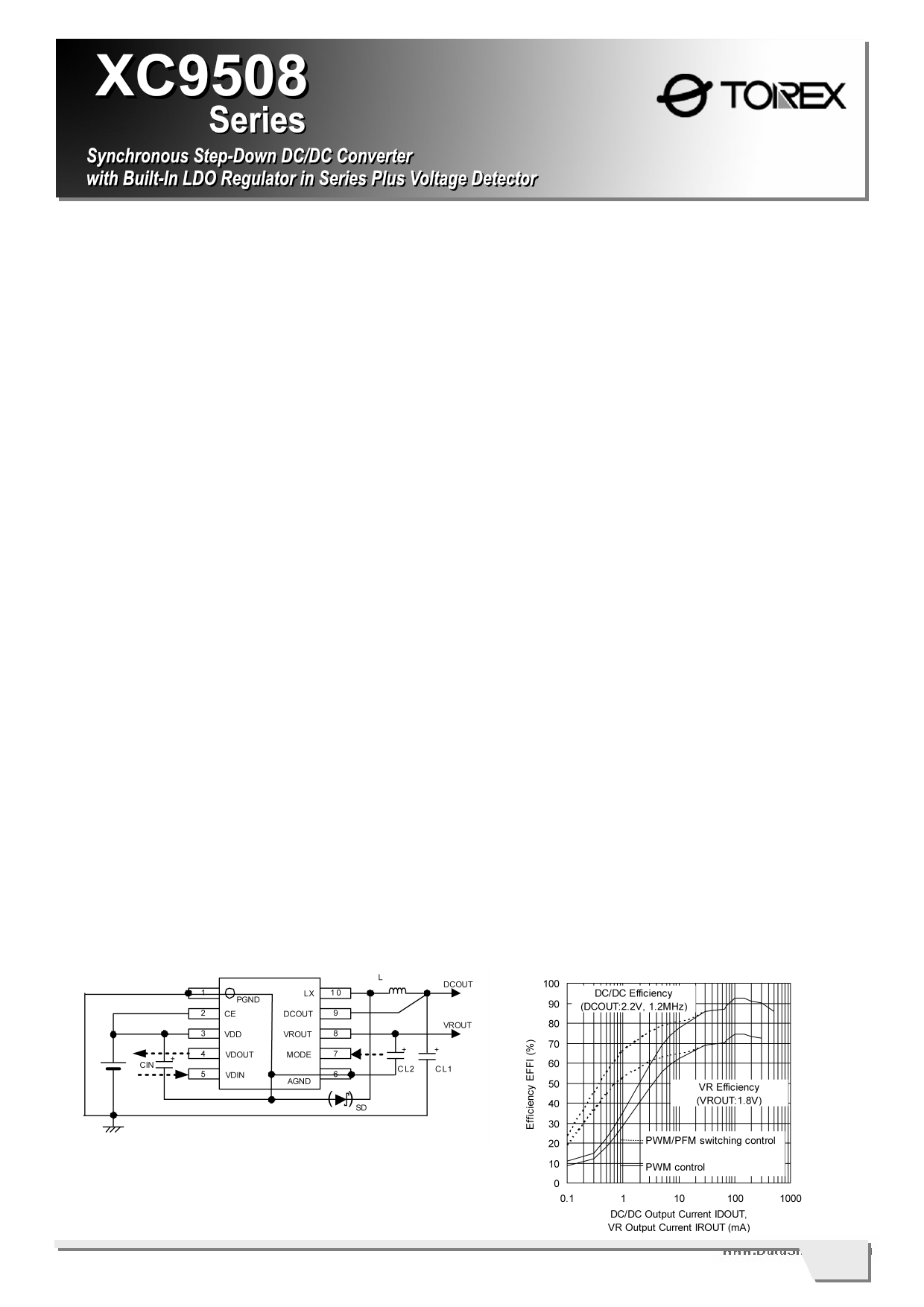
■TYPICAL APPLICATION CIRCUIT
■TYPICAL PERFORMANCE
CHARACTERISTICS
XC9508Cxxxx
VIN=3.6V, Topr=25OC
L=4.7μH (CDRH4D28C)
CIN:4.7μF ‘(ceramic), CL1:10μF (ceramic), CL2: 4.7μF (ceramic)
MSOP-10 (TOP VIEW)
* Please refer to the typical application circuit when external
components are selected.
Data Sheet
ud200541
1
1 page 
XC9508
Series
■ELECTRICAL CHARACTERISTICS
XC9508xxxCAx
●Common Characteristics
PARAMETER
Supply Current 1
Supply Current 2
Stand-by Current (*1)
Input Voltage Range
CE ‘H’ Level Voltage
CE ‘L’ Level Voltage
CE ‘H’ Level Current
CE ‘L’ Level Current
MODE 'H' Level Voltage*XC9508A
MODE 'H' Level Voltage*XC9508C
MODE 'L' Level Voltage*XC9508A
MODE 'L' Level Voltage*XC9508C
MODE 'H' Level Current
MODE 'L' Level Current
SYMBOL
IDD1
IDD2
ISTB
VIN
VCEH
VCEL
ICEH
ICEL
VMH
VMH
VML
VML
IMH
IML
CONDITIONS
VIN=CE=DCOUT=5.0V
VIN=CE=5.0V, DCOUT=0V
VIN=6.5V, CE=0V
MIN.
-
-
-
2.4
0.6
VSS
- 0.1
- 0.1
0.6
0.6
VSS
VSS
- 0.1
- 0.1
TYP.
250
300
0.5
-
-
-
-
-
-
-
-
-
-
-
MAX.
310
360
2.5
6.0
VDD
0.25
0.1
0.1
VDD
VDD
0.25
0.25
0.1
0.1
Topr=25℃
UNITS CIRCUIT
μA 1
μA 1
μA 1
V-
V3
V3
μA 1
μA 1
V2
V3
V2
V3
μA 1
μA 1
●DC/DC Converter (2.2V product)
PARAMETER
SYMBOL
Supply Current 1 *XC9508A
Supply Current 2 *XC9508A
PFM Supply Current 1 * 9508C
PFM Supply Current 2 * 9508C
IDD_DC1
IDD_DC2
IDD_PFM1
IDD_PFM2
Output Voltage
DCOUT(E)
Oscillation Frequency
FOSC
Maximum Duty Ratio
Minimum Duty Ratio
MAXDUTY
MINDUTY
PFM Duty Ratio
PFMDUTY
U.V.L.O. Voltage (*2)
LX SW ‘High’ ON Resistance (*3)
VUVLO
RLXH
LX SW ‘Low’ ON Resistance
RLXL
LX SW ‘High’ Leak Current (*12)
LX SW ‘Low’ Leak Current (*12)
Maximum Output Current
Current Limit (*9)
IleakH
IleakL
Imax1
Ilim1
Efficiency (*4)
EFFI
Output Voltage
Temperature Characteristics
U DCOUT
(UTopr・DCOUT)
Soft-Start Time
TSS
Latch Time (*5, 10)
Tlat
CONDITIONS
MIN.
VIN=CE=DCOUT=5.0V
-
VIN=CE=5.0V, DCOUT=0V
VIN=CE=DCOUT=5.0V
VIN=CE=5.0V, DCOUT=0V
Connected to the external components,
IDOUT=30mA
2.156
Connected to the external components,
1.02
IDOUT=10mA
DCOUT=0V
100
DCOUT=VIN
-
Connected to the external components,
No load
21
Connected to the external components 1.00
DCOUT=0V, LX=VIN-0.05V
-
Connected to the external components,
VIN=5.0V
-
VIN=LX=6.0V, CE=0V
-
VIN=6.0V, LX=CE=0V
-
Connected to the external components 600
1.0
Connected to the external components,
IDOUT=100mA
-
IDOUT=30mA
-40℃≦Topr≦85℃
-
Connected to the external components,
CE=0VtVIN, IDOUT=1mA
2
Connected to the external components,
VIN=CE=5.0V, Short DCOUT by 1Ω resistor
-
TYP.
200
250
250
300
2.200
1.20
-
-
30
1.40
0.5
0.5
0.05
0.05
-
1.1
90
±100
5
8
MAX.
280
330
310
360
2.244
1.38
-
0
38
1.78
0.9
0.9
1.00
1.00
-
-
-
-
10
25
Topr=25℃
UNITS CIRCUIT
μA 1
μA 1
μA 1
μA 1
V3
MHz
%
%
%
V
Ω
Ω
μA
μA
mA
A
%
ppm/
℃
mS
3
4
4
3
3
5
3
11
11
3
6
3
3
3
mS 10
Data Sheet
ud200541
5
5 Page 
XC9508
Series
■OPERATIONAL EXPLANATION (Continued)
●DC/DC Converter (Continued)
<Current Limit>
The current limiter circuit of the XC9508 series monitors the current flowing through the P-channel MOS driver transistor
connected to the Lx pin, and features a combination of the constant-current type current limit mode and the operation
suspension mode.
① When the driver current is greater than a specific level, the constant-current type current limit function operates to
turn off the pulses from the Lx pin at any given timing.
② When the driver transistor is turned off, the limiter circuit is then released from the current limit detection state.
③ At the next pulse, the driver transistor is turned on. However, the transistor is immediately turned off in the case of
an over current state.
④ When the over current state is eliminated, the IC resumes its normal operation.
The IC waits for the over current state to end by repeating the steps ① through ③ . If an over current state
continues for 8msec* and the above three steps are repeatedly performed, the IC performs the function of latching
the OFF state of the driver transistor, and goes into operation suspension mode. Once the IC is in suspension
mode, operations can be resumed by either turning the IC off via the CE/MODE pin, or by restoring power to the VIN
pin. The suspension mode does not mean a complete shutdown, but a state in which pulse output is suspended;
therefore, the internal circuitry remains in operation. The constant-current type current limit of the XC9508 series
can be set at 1.1A for MSOP-10 package and 0.7A for USP-10 package
<U.V.L.O. Circuit>
When the VIN pin voltage becomes 1.4 V or lower, the P-channel output driver transistor is forced OFF to prevent false
pulse output caused by unstable operation of the internal circuitry. When the VIN pin voltage becomes 1.8 V or higher,
switching operation takes place. By releasing the U.V.L.O. function, the IC performs the soft start function to initiate
output startup operation. The soft start function operates even when the VIN pin voltage falls momentarily below the
U.V.L.O. operating voltage. The U.V.L.O. circuit does not cause a complete shutdown of the IC, but causes pulse
output to be suspended; therefore, the internal circuitry remains in operation.
●High Speed LDO Voltage Regulator
The voltage regulator block of the XC9508 series consists of a reference voltage source, error amplifier, and current
limiter circuit. The voltage divided by split resistors is compared with the internal reference voltage by the error
amplifier. The P-channel MOSFET, which is connected to the VROUT pin, is then driven by the subsequent output
signal. The output voltage at the VROUT pin is controlled and stabilized by a system of negative feedback. A stable
output voltage is achievable even if used with low ESR capacitors as a phase compensation circuit is built-in.
<Reference Voltage Source>
The reference voltage source provides the reference voltage to ensure stable output voltage of the regulator.
<Error Amplifier>
The error amplifier compares the reference voltage with the signal from VROUT, and the amplifier controls the output of
the Pch driver transistor.
<Current Limit Circuit>
The voltage regulator block includes a combination of a constant current limiter circuit and a foldback circuit. When the
load current reaches the current limit level, the current limiter circuit operates and the output voltage of the voltage
regulator block drops. As a result of this drop in output voltage, the foldback circuit operates, output voltage drops
further and the load current decreases. When the VROUT and GND pin are shorted, the load current of about 30mA flows.
Data Sheet
ud200541
11
11 Page | ||
| Páginas | Total 30 Páginas | |
| PDF Descargar | [ Datasheet XC9508.PDF ] | |
Hoja de datos destacado
| Número de pieza | Descripción | Fabricantes |
| XC9500 | XC9500 In-System Programmable CPLD Family | Xilinx |
| XC9500XL | High-Performance CPLD | Xilinx |
| XC9501 | 2ch. Step-up DC/DC Controller ICs. | Torex Semiconductor |
| XC9502 | 2ch. Step-up / down DC/DC Controller ICs | Torex Semiconductor |
| Número de pieza | Descripción | Fabricantes |
| SLA6805M | High Voltage 3 phase Motor Driver IC. |
Sanken |
| SDC1742 | 12- and 14-Bit Hybrid Synchro / Resolver-to-Digital Converters. |
Analog Devices |
|
DataSheet.es es una pagina web que funciona como un repositorio de manuales o hoja de datos de muchos de los productos más populares, |
| DataSheet.es | 2020 | Privacy Policy | Contacto | Buscar |