|
|
PDF X28C512 Data sheet ( Hoja de datos )
| Número de pieza | X28C512 | |
| Descripción | (X28C512 / X28C513) Byte Alterable EEPROM | |
| Fabricantes | Intersil Corporation | |
| Logotipo |  |
|
Hay una vista previa y un enlace de descarga de X28C512 (archivo pdf) en la parte inferior de esta página. Total 21 Páginas | ||
|
No Preview Available !
®
Data Sheet
X28C512, X28C513
June 7, 2006
FN8106.2
5V, Byte Alterable EEPROM
The X28C512, X28C513 are 64K x 8 EEPROM, fabricated
with Intersil’s proprietary, high performance, floating gate
CMOS technology. Like all Intersil programmable nonvolatile
memories, the X28C512, X28C513 are 5V only devices. The
X28C512, X28C513 feature the JEDEC approved pin out for
byte wide memories, compatible with industry standard
EPROMS.
The X28C512, X28C513 support a 128-byte page write
operation, effectively providing a 39µs/byte write cycle and
enabling the entire memory to be written in less than 2.5
seconds. The X28C512, X28C513 also feature DATA Polling
and Toggle Bit Polling, system software support schemes
used to indicate the early completion of a write cycle. In
addition, the X28C512, X28C513 support the software data
protection option.
www.DataSheet4U.com
Features
• Access Time: 90ns
• Simple Byte and Page Write
- Single 5V supply
• No external high voltages or VPP control circuits
- Self-timed
• No erase before write
• No complex programming algorithms
• No overerase problem
• Low Power CMOS
- Active: 50mA
- Standby: 500µA
• Software Data Protection
- Protects data against system level inadvertent writes
• High Speed Page Write Capability
• Highly Reliable Direct Write™ Cell
- Endurance: 100,000 write cycles
- Data retention: 100 years
- Early end of write detection
- DATA polling
- Toggle bit polling
• Two PLCC and LCC Pinouts
- X28C512
• X28C010 EPROM pin compatible
- X28C513
• Compatible with lower density EEPROMs
• Pb-Free Plus Anneal Available (RoHS Compliant)
1 CAUTION: These devices are sensitive to electrostatic discharge; follow proper IC Handling Procedures.
1-888-INTERSIL or 1-888-468-3774 | Intersil (and design) is a registered trademark of Intersil Americas Inc.
Copyright Intersil Americas Inc. 2005, 2006. All Rights Reserved
All other trademarks mentioned are the property of their respective owners.
1 page 
X28C512, X28C513
Device Operation
Read
Read operations are initiated by both OE and CE LOW. The
read operation is terminated by either CE or OE returning
HIGH. This two line control architecture eliminates bus
contention in a system environment. The data bus will be in
a high impedance state when either OE or CE is HIGH.
Write
Write operations are initiated when both CE and WE are
LOW and OE is HIGH. The X28C512, X28C513 support
both a CE and WE controlled write cycle. That is, the
address is latched by the falling edge of either CE or WE,
whichever occurs last. Similarly, the data is latched internally
by the rising edge of either CE or WE, whichever occurs first.
A byte write operation, once initiated, will automatically
continue to completion, typically within 5ms.
Page Write Operation
The page write feature of the X28C512, X28C513 allows the
entire memory to be written in 2.5 seconds. Page write
allows two to one hundred twenty-eight bytes of data to be
consecutively written to the X28C512, X28C513, prior to the
commencement of the internal programming cycle. The host
can fetch data from another device within the system during
a page write operation (change the source address), but the
page address (A7 through A15) for each subsequent valid
write cycle to the part during this operation must be the same
as the initial page address.
The page write mode can be initiated during any write
operation. Following the initial byte write cycle, the host can
write an additional one to one hundred twenty-seven bytes in
the same manner as the first byte was written. Each
successive byte load cycle, started by the WE HIGH to LOW
transition, must begin within 100µs of the falling edge of the
preceding WE. If a subsequent WE HIGH to LOW transition
is not detected within 100µs, the internal automatic
programming cycle will commence. There is no page write
window limitation. Effectively, the page write window is
infinitely wide, so long as the host continues to access the
device within the byte load cycle time of 100µs.
Write Operation Status Bits
The X28C512, X28C513 provide the user two write
operation status bits. These can be used to optimize a
system write cycle time. The status bits are mapped onto the
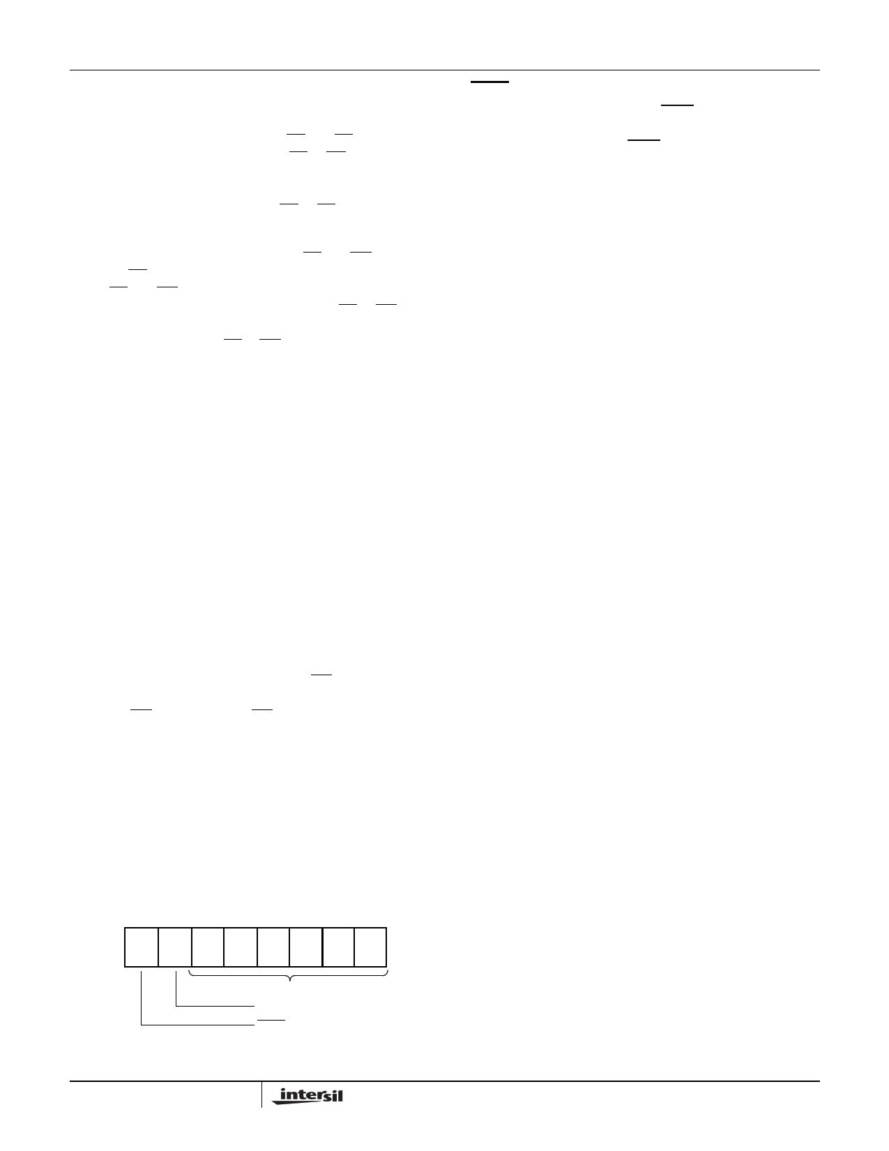
I/O bus as shown in Figure 1.
DATA Polling (I/O7)
The X28C512, X28C513 feature DATA polling as a method
to indicate to the host system that the byte write or page
write cycle has completed. DATA Polling allows a simple bit
test operation to determine the status of the X28C512,
X28C513, eliminating additional interrupt inputs or external
hardware. During the internal programming cycle, any
attempt to read the last byte written will produce the
complement of that data on I/O7 (i.e. write data = 0xxx xxxx,
read data = 1xxx xxxx). Once the programming cycle is
complete, I/O7 will reflect true data.
Toggle Bit (I/O6)
The X28C512, X28C513 also provide another method for
determining when the internal write cycle is complete. During
the internal programming cycle, I/O6 will toggle from HIGH to
LOW and LOW to HIGH on subsequent attempts to read the
device. When the internal cycle is complete, the toggling will
cease, and the device will be accessible for additional read
or write operations.
I/O DP TB 5 4 3 2 1 0
Reserved
Toggle Bit
DATA Polling
FIGURE 1. STATUS BIT ASSIGNMENT
5 FN8106.2
June 7, 2006
5 Page 
X28C512, X28C513
Absolute Maximum Ratings
Temperature under bias
X28C512, X28C513 . . . . . . . . . . . . . . . . . . . . . . . .-10°C to +85°C
X28C512I/513I . . . . . . . . . . . . . . . . . . . . . . . . . . .-65°C to +135°C
X28C512M/513M . . . . . . . . . . . . . . . . . . . . . . . . .-65°C to +135°C
Storage temperature . . . . . . . . . . . . . . . . . . . . . . . .-65°C to +150°C
Voltage on any pin with respect to VSS . . . . . . . . . . . . . . -1V to +7V
D.C. output current. . . . . . . . . . . . . . . . . . . . . . . . . . . . . . . . . . . 5mA
Lead temperature (soldering, 10s). . . . . . . . . . . . . . . . . . . . . . 300°C
Recommended Operating Conditions
Temperature Range
Commercial . . . . . . . . . . . . . . . . . . . . . . . . . . . . . . . 0°C to +70°C
Industrial. . . . . . . . . . . . . . . . . . . . . . . . . . . . . . . . .-40°C to +85°C
Military . . . . . . . . . . . . . . . . . . . . . . . . . . . . . . . . .-55°C to +125°C
Supply Voltage Limits . . . . . . . . . . . . . . . . . . . . . . . . . . . . .5V ±10%
CAUTION: Stresses above those listed under “Absolute Maximum Ratings” may cause permanent damage to the device. This is a stress rating only; functional
operation of the device (at these or any other conditions above those listed in the operational sections of this specification) is not implied. Exposure to absolute
maximum rating conditions for extended periods may affect device reliability.
DC Electrical Specifications Over recommended operating conditions, unless otherwise specified.
SYMBOL
PARAMETER
TEST CONDITIONS
ICC VCC current (active) (TTL inputs)
CE = OE = VIL, WE = VIH, All I/O’s = open, address
inputs = 0.4V/2.4V Levels @ f = 5MHz
ISB1
ISB2
VCC current (standby) (TTL inputs)
VCC current (standby) (CMOS inputs)
ILI
ILO
VlL
(Note 1)
Input leakage current
Output leakage current
Input LOW voltage
CE = VIH, OE = VIL, All I/O’s = open, other inputs = VIH
CE = VCC - 0.3V, OE = VIL, All I/O’s = Open, Other Inputs
= VIH
VIN = VSS to VCC
VOUT = VSS to VCC, CE = VIH
VIH Input HIGH voltage
(Note 1)
VOL Output LOW voltage
IOL = 2.1mA
VOH Output HIGH voltage
IOH = -400µA
NOTE:
1. VIL min. and VIH max. are for reference only and are not tested.
MIN
-1
2
2.4
MAX
50
UNIT
mA
3 mA
500 µA
10 µA
10 µA
0.8 V
VCC + 1
0.4
V
V
V
Power-Up Timing
SYMBOL
PARAMETER
tPUR (Note 2)
tPUW (Note 2)
Power-up to read operation
Power-up to write operation
MAX
100
5
UNIT
µs
ms
Capacitance TA = +25°C, f = 1MHz, VCC = 5V
SYMBOL
PARAMETER
CI/O (Note 2)
CIN (Note 2)
Input/output capacitance
Input capacitance
TEST CONDITIONS
VI/O = 0V
VIN = 0V
MAX
10
10
UNIT
pF
pF
Endurance and Data Retention
PARAMETER
Endurance
Endurance
Data retention
MIN
10,000
100,000
100
MAX
UNIT
Cycles per byte
Cycles per page
Years
NOTE:
2. This parameter is periodically sampled and not 100% tested.
11 FN8106.2
June 7, 2006
11 Page | ||
| Páginas | Total 21 Páginas | |
| PDF Descargar | [ Datasheet X28C512.PDF ] | |
Hoja de datos destacado
| Número de pieza | Descripción | Fabricantes |
| X28C512 | 5 Volt/ Byte Alterable E2PROM | Xicor |
| X28C512 | (X28C512 / X28C513) Byte Alterable EEPROM | Intersil Corporation |
| X28C512D-12 | 5 Volt/ Byte Alterable E2PROM | Xicor |
| X28C512D-15 | 5 Volt/ Byte Alterable E2PROM | Xicor |
| Número de pieza | Descripción | Fabricantes |
| SLA6805M | High Voltage 3 phase Motor Driver IC. |
Sanken |
| SDC1742 | 12- and 14-Bit Hybrid Synchro / Resolver-to-Digital Converters. |
Analog Devices |
|
DataSheet.es es una pagina web que funciona como un repositorio de manuales o hoja de datos de muchos de los productos más populares, |
| DataSheet.es | 2020 | Privacy Policy | Contacto | Buscar |
