|
|
|
PDF HIP6521 Data sheet ( Hoja de datos )
| Número de pieza | HIP6521 | |
| Descripción | PWM and Triple Linear Power Controller | |
| Fabricantes | Intersil Corporation | |
| Logotipo | ||
Hay una vista previa y un enlace de descarga de HIP6521 (archivo pdf) en la parte inferior de esta página. Total 13 Páginas | ||
|
No Preview Available !
®
Data Sheet
October 16, 2006
HIP6521
FN4837.5
PWM and Triple Linear Power Controller
The HIP6521 provides the power control and protection for
four output voltages in high-performance microprocessor and
computer applications. The IC integrates a voltage-mode
PWM controller and three linear controllers, as well as
monitoring and protection functions into a 16 Ld SOIC
package. The PWM controller is intended to regulate the
microprocessor memory core voltage with a
synchronous-rectified buck converter. The linear controllers
are intended to regulate the computer system’s AGP 1.5V bus
power, the 2.5V clock power, and the 1.8V power for the
North/South Bridge core voltage and/or cache memory
circuits. Both the switching regulator and linear voltage
references provide ±2% of static regulation over line, load,
and temperature ranges. All outputs are user-adjustable by
means of an external resistor divider. All linear controllers
employ bipolar NPNs for the pass transistors.
The HIP6521 monitors all the output voltages. The PWM
controller’s adjustable overcurrent function monitors the
output current by using the voltage drop across the upper
MOSFET’s rDS(ON). The linear regulator outputs are
monitored via the FB pins for undervoltage events.
Orderingwww.DataSheet4U.com Information
PART
NUMBER
PART
TEMP.
PKG.
MARKING RANGE (°C) PACKAGE DWG. #
HIP6521CB HIP6521CB 0 to 70 16 Ld SOIC M16.15
HIP6521CBZ 6521CBZ
(Note)
0 to 70
16 Ld SOIC M16.15
(Pb-free)
HIP6521EVAL1 Evaluation Board
NOTE: Intersil Pb-free plus anneal products employ special Pb-free
material sets; molding compounds/die attach materials and 100%
matte tin plate termination finish, which are RoHS compliant and
compatible with both SnPb and Pb-free soldering operations. Intersil
Pb-free products are MSL classified at Pb-free peak reflow
temperatures that meet or exceed the Pb-free requirements of
IPC/JEDEC J STD-02.
Add “-T” suffix for tape and reel.
Features
• Provides 4 Regulated Voltages
- Memory Core, AGP, Clock, and Memory Controller Hub
Power
• ACPI Compatible
• Drives Bipolar Linear Pass Transistors
• Externally Resistor-Adjustable Outputs
• Simple Single-Loop Control Design
- Voltage-Mode PWM Control
• Fast PWM Converter Transient Response
- High-Bandwidth Error Amplifier
- Full 0% to 100% Duty Ratio
• Excellent Output Voltage Regulation
- All Outputs: ±2% Over Temperature
• Overcurrent Fault Monitors
- Switching Regulator Does Not Require Extra Current
Sensing Element, Uses MOSFET’s rDS(ON)
• Small Converter Size
- 300kHz Constant Frequency Operation
- Small External Component Count
• Pb-Free Plus Anneal Available (RoHS Compliant)
Applications
• Motherboard Power Regulation for Computers
Related Literature
• Technical Brief TB363 “Guidelines for Handling and
Processing Moisture Sensitive Surface Mount Devices
(SMDs)”
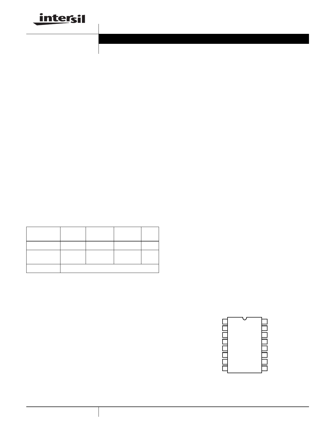
Pinout
HIP6521 (SOIC)
TOP VIEW
DRIVE2 1
FB2 2
FB 3
COMP 4
GND 5
PHASE 6
BOOT 7
UGATE 8
16 FB3
15 DRIVE3
14 FB4
13 DRIVE4
12 OCSET
11 VCC
10 LGATE
9 PGND
1
CAUTION: These devices are sensitive to electrostatic discharge; follow proper IC Handling Procedures.
1-888-INTERSIL or 1-888-468-3774 | Intersil (and design) is a registered trademark of Intersil Americas Inc.
Copyright © Intersil Americas Inc. 2000, 2004, 2006. All Rights Reserved
All other trademarks mentioned are the property of their respective owners.
1 page 
HIP6521
Functional Pin Descriptions
VCC (Pin 11)
Provide a well decoupled 5V bias supply for the IC to this
pin. This pin also provides the gate bias charge for the lower
MOSFET controlled by the PWM section of the IC, as well as
the base current drive for the linear regulators’ external
bipolar transistors. The voltage at this pin is monitored for
Power-On Reset (POR) purposes.
GND (Pin 5)
Signal ground for the IC. All voltage levels are measured
with respect to this pin.
PGND (Pin 9)
This is the power ground connection. Tie the synchronous
PWM converter’s lower MOSFET source to this pin.
BOOT (Pin 7)
Connect a suitable capacitor (0.47µF recommended) from
this pin to PHASE. This bootstrap capacitor supplies UGATE
driver the energy necessary to turn and hold the upper
MOSFET on.
OCSET (Pin 12)
Connect a resistor from this pin to the drain of the upper
PWM MOSFET. This resistor, an internal 40µA current
source (typical), and the upper MOSFET’s on-resistance set
the converter overcurrent trip point. An overcurrent trip
cycles the soft-start function.
The voltage at this pin is monitored for power-on reset (POR)
purposes and pulling this pin below 1.25V with an open
drain/collector device will shutdown the switching controller.
PHASE (Pin 6)
Connect the PHASE pin to the PWM converter’s upper
MOSFET source. This pin is used to monitor the voltage
drop across the upper MOSFET for overcurrent protection.
UGATE (Pin 8)
Connect UGATE pin to the PWM converter’s upper MOSFET
gate. This pin provides the gate drive for the upper MOSFET.
LGATE (Pin 10)
Connect LGATE to the PWM converter’s lower MOSFET
gate. This pin provides the gate drive for the lower MOSFET.
COMP and FB (Pins 4, 3)
COMP and FB are the available external pins of the PWM
converter error amplifier. The FB pin is the inverting input of the
error amplifier. Similarly, the COMP pin is the error amplifier
output. These pins are used to compensate the voltage-mode
control feedback loop of the synchronous PWM converter.
DRIVE2, 3, 4 (Pins 1, 15, 13)
Connect these pins to the base terminals of external bipolar
NPN transistors. These pins provide the base current drive
for the regulator pass transistors.
FB2, 3, 4 (Pins 2, 16, 14)
Connect the output of the corresponding linear regulators to
these pins through properly sized resistor dividers. The
voltage at these pins is regulated to 0.8V. These pins are
also monitored for undervoltage events.
Quickly pulling and holding any of these pins above 1.25V
(using diode-coupled logic devices) shuts off the respective
regulators. Releasing these pins from the pull-up voltage
initiates a soft-start sequence on the respective regulator.
Description
Operation
The HIP6521 monitors and precisely controls 4 output
voltage levels (Refer to Block and Simplified Power System
Diagrams, and Typical Application Schematic). It is
designed for microprocessor computer applications with
3.3V, and 5V (5VDUAL) bias input from an ATX power
supply. The IC has a synchronous PWM controller and
three linear controllers. The PWM controller (PWM) is
designed to regulate the 2.5V memory voltage (VOUT1).
The PWM controller drives 2 MOSFETs (Q1 and Q2) in a
synchronous-rectified buck converter configuration and
regulates the output voltage to a level programmed by a
resistor divider. The linear controllers are designed to
regulate three more of the computer system’s voltages,
typically the 1.5V AGP bus (VOUT4), the 2.5V clock voltage
(VOUT2), and the 1.8V ICH/MCH core voltage (VOUT3). All
linear controllers are designed to employ external NPN
bipolar pass transistors.
Initialization
The HIP6521 automatically initializes upon receipt of input
power. Special sequencing of the input supplies is not
necessary. The Power-On Reset (POR) function continually
monitors the input bias supply voltage. The POR monitors
the bias voltage at the VCC pin. The POR function initiates
soft-start operation after the bias supply voltage exceeds its
POR threshold.
Soft-Start
The POR function initiates the soft-start sequence. The
PWM error amplifier reference input is clamped to a level
proportional to the soft-start voltage. As the soft-start voltage
slews up, the PWM comparator generates PHASE pulses of
increasing width that charge the output capacitor(s).
Similarly, all linear regulators’ reference inputs are clamped
to a voltage proportional to the soft-start voltage. The
ramp-up of the internal soft-start function provides a
controlled output voltage rise.
Figure 1 shows the soft-start sequence for the typical
application. At T0 the +5VSB bias voltage starts to ramp up
(closely followed by the +5VDUAL voltage) crossing the 4.5V
POR threshold at time T1. On the PWM section, the oscillator’s
triangular waveform is compared to the clamped error amplifier
5 FN4837.5
October 16, 2006
5 Page 
HIP6521
Use a mix of input bypass capacitors to control the voltage
overshoot across the MOSFETs. Use ceramic capacitance
for the high frequency decoupling and bulk capacitors to
supply the RMS current. Small ceramic capacitors can be
placed very close to the upper MOSFET to suppress the
voltage induced in the parasitic circuit impedances.
For a through-hole design, several electrolytic capacitors
may be needed. For surface mount designs, solid tantalum
capacitors can be used, but caution must be exercised with
regard to the capacitor surge current rating. These
capacitors must be capable of handling the surge-current at
power-up.
Transistors Selection/Considerations
The HIP6521 requires 5 external transistors. Two N-channel
MOSFETs are used in the synchronous-rectified buck
topology of PWM converter. The clock, AGP and MCH/ICH
linear controllers each drive an NPN bipolar transistor as a
pass element. All these transistors should be selected based
upon rDS(ON) , current gain, saturation voltages, gate/base
supply requirements, and thermal management
considerations.
PWM MOSFET Selection and Considerations
In high-current PWM applications, the MOSFET power
dissipation, package selection and heatsink are the
dominant design factors. The power dissipation includes two
loss components; conduction loss and switching loss. These
losses are distributed between the upper and lower
MOSFETs according to duty factor (see the equations
below). The conduction losses are the main component of
power dissipation for the lower MOSFETs. Only the upper
MOSFET has significant switching losses, since the lower
device turns on and off into near zero voltage.
The equations below assume linear voltage-current
transitions and do not model power loss due to the reverse-
recovery of the lower MOSFET’s body diode. The gate-
charge losses are dissipated by the HIP6521 and don't heat
the MOSFETs. However, large gate-charge increases the
switching time, tSW which increases the upper MOSFET
switching losses. Ensure that both MOSFETs are within their
maximum junction temperature at high ambient temperature
by calculating the temperature rise according to package
thermal-resistance specifications. A separate heatsink may
be necessary depending upon MOSFET power, package
type, ambient temperature and air flow.
PUPPER = I--O-----2----×-----r--D----S----V(--O--I--N-N----)---×-----V----O-----U----T-- + I--O------×-----V----I--N-----×-2----t--S----W------×-----F----S--
PLOWER = I--O-----2----×-----r--D----S----(--O-----N---V-)---×I--N---(---V----I--N-----–----V-----O----U----T----)
Given the reduced available gate bias voltage (5V) logic-
level or sub-logic-level transistors have to be used for both
N-MOSFETs. Caution should be exercised with devices
exhibiting very low VGS(ON) characteristics, as the low gate
threshold could be conducive to some shoot-through (due to
the Miller effect), in spite of the counteracting circuitry
present aboard the HIP6521.
+5V
VCC
HIP6521
BOOT
CBOOT
UGATE
PHASE
VCC
+- LGATE
PGND
GND
+5V OR LESS
+
Q1
NOTE:
VGS ≈ VCC -0.5V
Q2 CR1
NOTE:
VGS ≈ VCC
FIGURE 8. MOSFET GATE BIAS
Rectifier CR1 is a clamp that catches the negative inductor
swing during the dead time between the turn off of the lower
MOSFET and the turn on of the upper MOSFET. The diode
must be a Schottky type to prevent the lossy parasitic
MOSFET body diode from conducting. It is acceptable to
omit the diode and let the body diode of the lower MOSFET
clamp the negative inductor swing, providing the body diode
is fast enough to avoid excessive negative voltage swings at
the PHASE pin. The diode's rated reverse breakdown
voltage must be greater than the maximum input voltage.
Linear Controllers Transistor Selection
The main criteria for selection of transistors for the linear
regulators is package selection for efficient removal of heat.
The power dissipated in a linear regulator is:
PLINEAR = IO × (VIN – VOUT)
Select a package and heatsink that maintains the junction
temperature below the rating with a the maximum expected
ambient temperature.
As bipolar NPN transistors have to be used with the linear
controllers, insure the current gain at the given operating
VCE is sufficiently large to provide the desired maximum
output load current when the base is fed with the minimum
driver output current.
11 FN4837.5
October 16, 2006
11 Page | ||
| Páginas | Total 13 Páginas | |
| PDF Descargar | [ Datasheet HIP6521.PDF ] | |
Hoja de datos destacado
| Número de pieza | Descripción | Fabricantes |
| HIP6521 | PWM and Triple Linear Power Controller | Intersil Corporation |
| Número de pieza | Descripción | Fabricantes |
| SLA6805M | High Voltage 3 phase Motor Driver IC. |
Sanken |
| SDC1742 | 12- and 14-Bit Hybrid Synchro / Resolver-to-Digital Converters. |
Analog Devices |
|
DataSheet.es es una pagina web que funciona como un repositorio de manuales o hoja de datos de muchos de los productos más populares, |
| DataSheet.es | 2020 | Privacy Policy | Contacto | Buscar |