|
|
PDF HI5662 Data sheet ( Hoja de datos )
| Número de pieza | HI5662 | |
| Descripción | 60MSPS A/D Converter | |
| Fabricantes | Intersil Corporation | |
| Logotipo |  |
|
Hay una vista previa y un enlace de descarga de HI5662 (archivo pdf) en la parte inferior de esta página. Total 14 Páginas | ||
|
No Preview Available !
Data Sheet
HI5662
February 1999 File Number 4317.2
Dual 8-Bit, 60MSPS A/D Converter with
Internal Voltage Reference
The HI5662 is a monolithic, dual 8-Bit, 60MSPS analog-to-
digital converter fabricated in an advanced CMOS process.
It is designed for high speed applications where integration,
bandwidth and accuracy are essential. The HI5662 reaches
a new level of multi-channel integration. The fully pipeline
architecture and an innovative input stage enable the HI5662
to accept a variety of input configurations, single-ended or
fully differential. Only one external clock is necessary to
drive both converters and an internal band-gap voltage
reference is provided. This allows the system designer to
realize an increased level of system integration resulting in
decreased cost and power dissipation.
The HI5662 has excellent dynamic performance while
consuming only 650mW power at 60MSPS. The A/D only
requires a single +5V power supply and encode clock. Data
output latches are provided which present valid data to the
output bus with a latency of 6 clock cycles.
For those customers needing dual channel 10-bit resolution,
please refer to the HI5762. For single channel 10-bit
applications, please refer to the HI5767.
www.DataSheet4U.com
Ordering Information
PART
NUMBER
HI5662/6IN
HI5662EVAL2
TEMP.
RANGE (oC)
PACKAGE
PKG. NO.
-40 to 85 44 Ld MQFP
Q44.10x10
25 Evaluation Platform
Features
• Sampling Rate . . . . . . . . . . . . . . . . . . . . . . . . . . .60MSPS
• 7.8 Bits at fIN = 10MHz
• Low Power at 60MSPS. . . . . . . . . . . . . . . . . . . . . 650mW
• Wide Full Power Input Bandwidth. . . . . . . . . . . . . 250MHz
• Excellent Channel-to-Channel Isolation . . . . . . . . . >75dB
• On-Chip Sample and Hold Amplifiers
• Internal Band-Gap Voltage Reference . . . . . . . . . . . . 2.5V
• Fully Differential or Single-Ended Analog Inputs
• Single Supply Voltage Operation . . . . . . . . . . . . . . . . +5V
• TTL/CMOS Compatible Digital Inputs
• CMOS Compatible Digital Outputs . . . . . . . . . . . . 3.0/5.0V
• Offset Binary Digital Data Output Format
• Dual 8-Bit A/D Converters on a Monolithic Chip
Applications
• Wireless Local Loop
• PSK and QAM I and Q Demodulators
• Medical Imaging
• High Speed Data Acquisition
Pinout
HI5662
(MQFP)
TOP VIEW
AGND
AVCC2
ID7
ID6
ID5
ID4
ID3
DVCC3
DGND
ID2
ID1
44 43 42 41 40 39 38 37 36 35 34
1 33
2 32
3 31
4 30
5 29
6 28
7 27
8 26
9 25
10 24
11 23
12 13 14 15 16 17 18 19 20 21 22
AGND
AVCC2
QD7
QD6
QD5
QD4
QD3
DVCC3
DGND
QD2
QD1
10 CAUTION: These devices are sensitive to electrostatic discharge; follow proper IC Handling Procedures.
1-888-INTERSIL or 321-724-7143 | Copyright © Intersil Corporation 1999
1 page 
HI5662
Absolute Maximum Ratings TA = 25oC
Supply Voltage, AVCC or DVCC to AGND or DGND . . . . . . . . . . .6V
DGND to AGND . . . . . . . . . . . . . . . . . . . . . . . . . . . . . . . . . . . . . . . . 0.3V
Digital I/O Pins . . . . . . . . . . . . . . . . . . . . . . . . . . . . . DGND to DVCC
Analog I/O Pins . . . . . . . . . . . . . . . . . . . . . . . . . . . . AGND to AVCC
Operating Conditions
Temperature Range
HI5662/6IN . . . . . . . . . . . . . . . . . . . . . . . . . . . . . . . -40oC to 85oC
Thermal Information
Thermal Resistance (Typical, Note 1)
θJA (oC/W)
HI5662/6IN . . . . . . . . . . . . . . . . . . . . . . . . . . . . . . . .
75
Maximum Junction Temperature . . . . . . . . . . . . . . . . . . . . . . .150oC
Maximum Storage Temperature Range . . . . . . . . . . -65oC to 150oC
Maximum Lead Temperature (Soldering 10s) . . . . . . . . . . . . .300oC
(Lead Tips Only)
CAUTION: Stresses above those listed in “Absolute Maximum Ratings” may cause permanent damage to the device. This is a stress only rating and operation of the
device at these or any other conditions above those indicated in the operational sections of this specification is not implied.
NOTE:
1. θJA is measured with the component mounted on an evaluation PC board in free air.
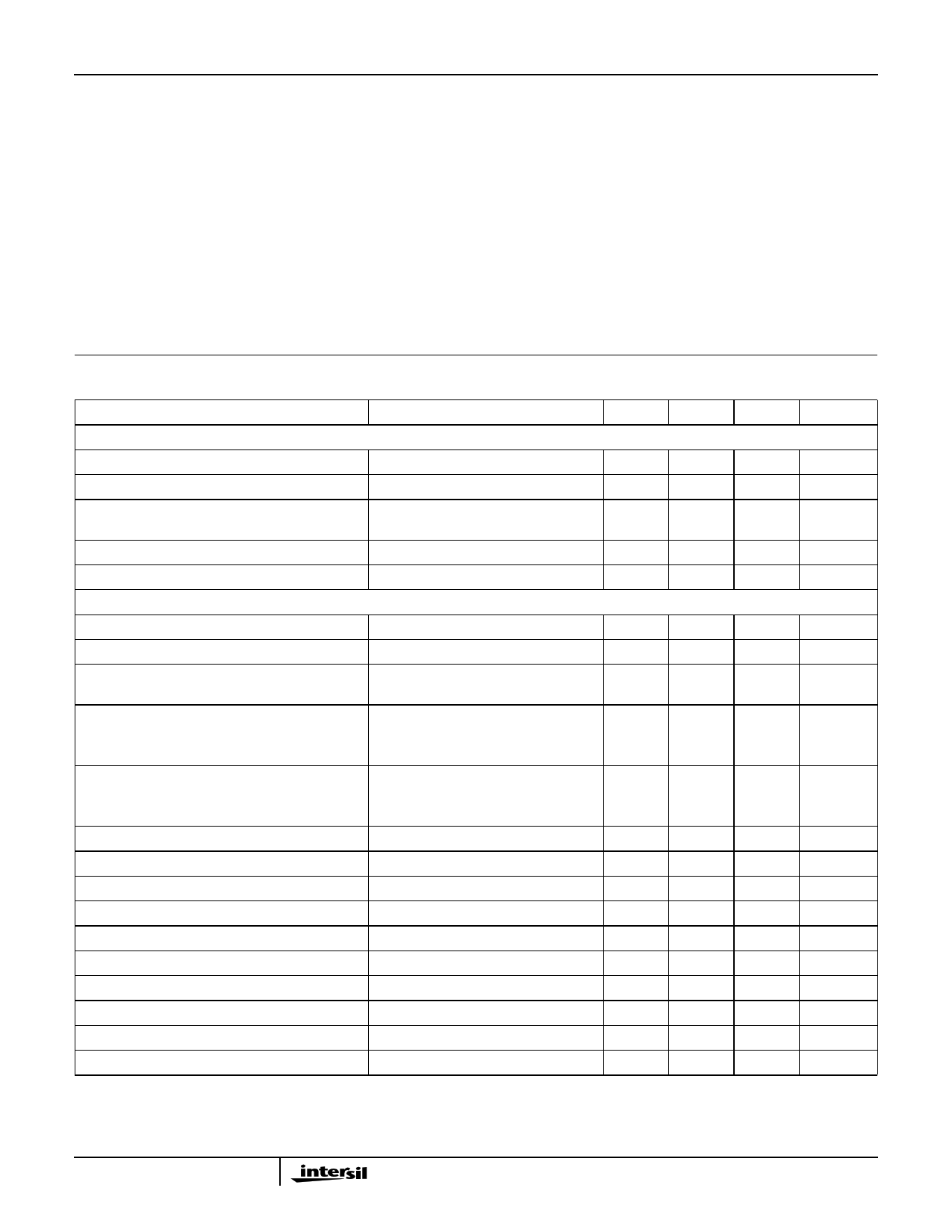
Electrical Specifications AVCC1,2 = DVCC1,2 = +5.0V, DVCC3 = +3.0V; VRIN = 2.50V; fS = 60MSPS at 50% Duty Cycle;
CL = 10pF; TA = 25oC; Differential Analog Input; Unless Otherwise Specified
PARAMETER
TEST CONDITIONS
MIN TYP MAX
ACCURACY
Resolution
8- -
Integral Linearity Error, INL
Differential Linearity Error, DNL
(Guaranteed No Missing Codes)
fIN = 10MHz
fIN = 10MHz
- 0.5 -
- ±0.2 ±1.0
Offset Error, VOS
Full Scale Error, FSE
DYNAMIC CHARACTERISTICS
fIN = DC
fIN = DC
-10 - +10
-1-
Minimum Conversion Rate
No Missing Codes
-1-
Maximum Conversion Rate
No Missing Codes
60 -
-
Effective Number of Bits, ENOB
Signal to Noise and Distortion Ratio, SINAD
= R-----M-----S------NR----oM---i--sS---e---S--+--i-g--D--n--i-as---lt--o---r--t--i-o----n-
fIN = 10MHz
fIN = 10MHz, Single Ended Analog Input
fIN = 10MHz
7.5
7.0
-
7.8
7.7
48.7
-
-
-
Signal to Noise Ratio, SNR
= R-R----M-M----S-S-----SN----i-og---in-s---ae---l
fIN = 10MHz
- 48 -
Total Harmonic Distortion, THD
2nd Harmonic Distortion
3rd Harmonic Distortion
Spurious Free Dynamic Range, SFDR
Intermodulation Distortion, IMD
I/Q Channel Crosstalk
I/Q Channel Offset Match
I/Q Channel Full Scale Error Match
Transient Response
Over-Voltage Recovery
fIN = 10MHz
fIN = 10MHz
fIN = 10MHz
fIN = 10MHz
f1 = 1MHz, f2 = 1.02MHz
(Note 2)
0.2V Overdrive (Note 2)
- -66 -
- -71 -
- -71 -
- 71 -
- 64 -
- -75 -60
- 2.5 -
- 2.5 -
-1-
-1-
UNITS
Bits
LSB
LSB
LSB
LSB
MSPS
MSPS
Bits
Bits
dB
dB
dBc
dBc
dBc
dBc
dBc
dBc
LSB
LSB
Cycle
Cycle
14
5 Page 
HI5662
TABLE 1. A/D CODE TABLE
CODE CENTER
DESCRIPTION
+Full Scale (+FS) -7/16LSB
+FS - 17/16LSB
+9/16LSB
-7/16LSB
-FS + 19/16LSB
-Full Scale (-FS) + 9/16LSB
DIFFERENTIAL INPUT
VOLTAGE
(I/QIN+ - I/QIN-)
0.498291V
0.494385V
2.19727mV
-1.70898mV
-0.493896V
-0.497803V
OFFSET BINARY OUTPUT CODE
MSB
I/QD7 I/QD6 I/QD5 I/QD4 I/QD3 I/QD2 I/QD1
1111111
1111111
1000000
0111111
0000000
0000000
NOTE:
8. The voltages listed above represent the ideal center of each output code shown with VREFIN = +2.5V.
LSB
I/QD0
1
0
0
1
1
0
Detailed Description
Theory of Operation
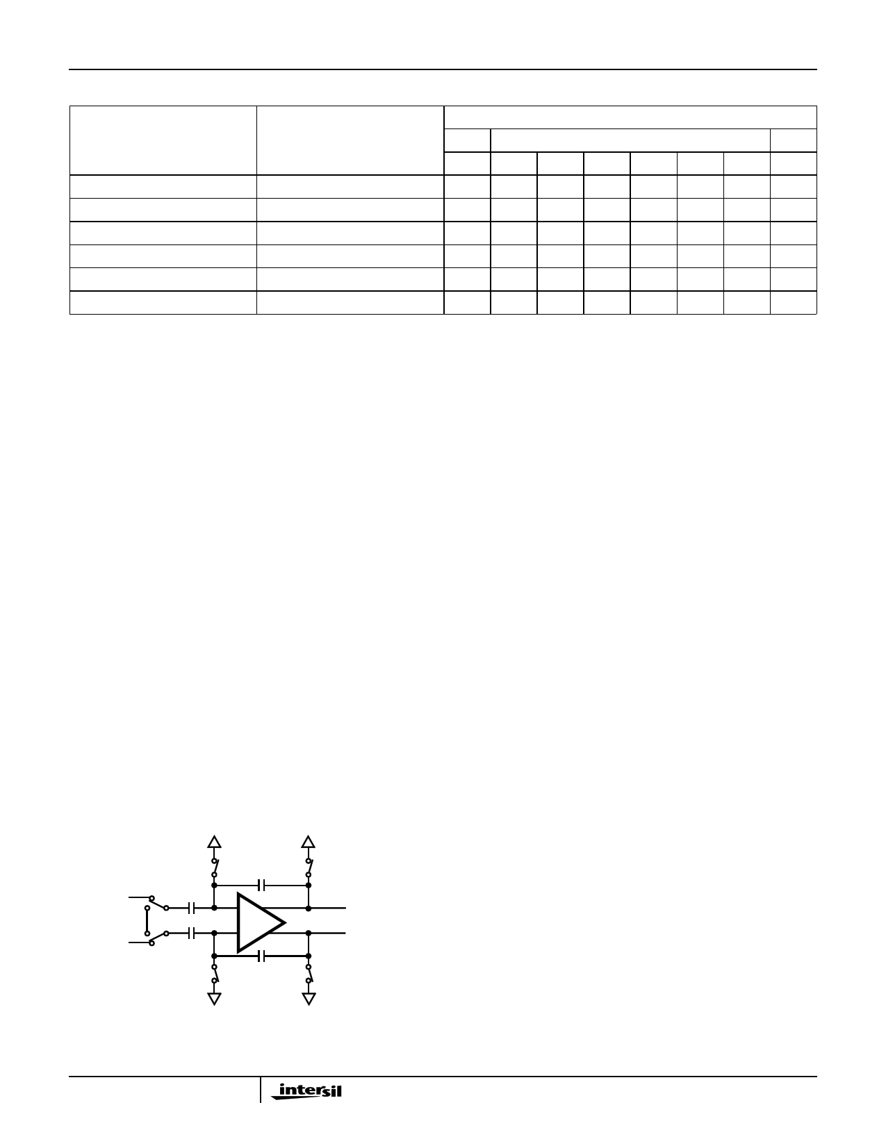
The HI5662 is a dual 8-bit fully differential sampling pipeline
A/D converter with digital error correction logic. Figure 14
depicts the circuit for the front end differential-in-differential-
out sample-and-hold (S/H) amplifiers. The switches are
controlled by an internal sampling clock which is a non-
overlapping two phase signal, φ1 and φ2, derived from the
master sampling clock. During the sampling phase, φ1, the
input signal is applied to the sampling capacitors, CS. At the
same time the holding capacitors, CH, are discharged to
analog ground. At the falling edge of φ1 the input signal is
sampled on the bottom plates of the sampling capacitors. In
the next clock phase, φ2, the two bottom plates of the
sampling capacitors are connected together and the holding
capacitors are switched to the op-amp output nodes. The
charge then redistributes between CS and CH completing
one sample-and-hold cycle. The front end sample-and-hold
output is a fully-differential, sampled-data representation of
the analog input. The circuit not only performs the sample-
and-hold function but will also convert a single-ended input
to a fully-differential output for the converter core. During the
sampling phase, the I/QIN pins see only the on-resistance of
a switch and CS. The relatively small values of these
components result in a typical full power input bandwidth of
250MHz for the converter.
I/QIN+
I/QIN-
Φ1
Φ2
Φ1
Φ1
CS
CS
Φ1
CH
-+
+-
CH
Φ1
VOUT+
VOUT-
Φ1
FIGURE 14. ANALOG INPUT SAMPLE-AND-HOLD
As illustrated in the functional block diagram and the timing
diagram in Figure 1, identical pipeline subconverter stages,
each containing a two-bit flash converter and a two-bit
multiplying digital-to-analog converter, follow the S/H circuit
with the last stage being a two bit flash converter. Each
converter stage in the pipeline will be sampling in one phase
and amplifying in the other clock phase. Each individual
subconverter clock signal is offset by 180 degrees from the
previous stage clock signal resulting in alternate stages in
the pipeline performing the same operation.
The output of each of the identical two-bit subconverter
stages is a two-bit digital word containing a supplementary
bit to be used by the digital error correction logic. The output
of each subconverter stage is input to a digital delay line
which is controlled by the internal sampling clock. The
function of the digital delay line is to time align the digital
outputs of the identical two-bit subconverter stages with the
corresponding output of the last stage flash converter before
applying the results to the digital error correction logic. The
digital error correction logic uses the supplementary bits to
correct any error that may exist before generating the final
eight bit digital data output of the converter.
Because of the pipeline nature of this converter, the digital
data representing an analog input sample is output to the
digital data bus following the 6th cycle of the clock after the
analog sample is taken (see the timing diagram in Figure 1).
This time delay is specified as the data latency. After the
data latency time, the digital data representing each
succeeding analog sample is output during the following
clock cycle. The digital output data is provided in offset
binary format (see Table 1, A/D Code Table).
Internal Reference Voltage Output, VREFOUT
The HI5662 is equipped with an internal reference voltage
generator, therefore, no external reference voltage is
required. VROUT must be connected to VRIN when using the
internal reference voltage.
20
11 Page | ||
| Páginas | Total 14 Páginas | |
| PDF Descargar | [ Datasheet HI5662.PDF ] | |
Hoja de datos destacado
| Número de pieza | Descripción | Fabricantes |
| HI5660 | High Speed D/A Converter | Intersil Corporation |
| HI5662 | 60MSPS A/D Converter | Intersil Corporation |
| HI5667 | 60MSPS A/D Converter | Intersil Corporation |
| Número de pieza | Descripción | Fabricantes |
| SLA6805M | High Voltage 3 phase Motor Driver IC. |
Sanken |
| SDC1742 | 12- and 14-Bit Hybrid Synchro / Resolver-to-Digital Converters. |
Analog Devices |
|
DataSheet.es es una pagina web que funciona como un repositorio de manuales o hoja de datos de muchos de los productos más populares, |
| DataSheet.es | 2020 | Privacy Policy | Contacto | Buscar |
