|
|
|
PDF HI5960 Data sheet ( Hoja de datos )
| Número de pieza | HI5960 | |
| Descripción | High Speed D/A Converter | |
| Fabricantes | Intersil Corporation | |
| Logotipo | ||
Hay una vista previa y un enlace de descarga de HI5960 (archivo pdf) en la parte inferior de esta página. Total 12 Páginas | ||
|
No Preview Available !
®
Data Sheet
March 31, 2005
HI5960
FN4655.6
14-Bit, 130MSPS, High Speed D/A
Converter
The HI5960 is a 14-bit, 130MSPS (Mega Samples Per
Second), high speed, low power, D/A converter which is
implemented in an advanced CMOS process. Operating
from a single +3V to +5V supply, the converter provides
20mA of full scale output current and includes edge-
triggered CMOS input data latches. Low glitch energy and
excellent frequency domain performance are achieved using
a segmented current source architecture.
This device complements the HI5x60 and HI5x28 family of
high speed converters, which includes 8, 10, 12, and 14-bit
devices.
Ordering Information
PART
NUMBER
HI5960IB
HI5960IBZ
(See Note)
TEMP.
RANGE
(oC)
PACKAGE
PKG. CLOCK
DWG. # SPEED
-40 to 85 28 Ld SOIC M28.3 130MHz
-40 to 85 28 Ld SOIC M28.3
(Pb-free)
130MHz
HI5960IA
-40 to 85 28 Ld TSSOP M28.173 130MHz
HI5960IAZ
(See Note)
-40 to 85 28 Ld TSSOP M28.173 130MHz
(Pb-free)
HI5960IA-T
-40 to 85 28 Ld TSSOP M28.173 130MHz
Tape and Reel
HI5960IAZ-T
(See Note)
-40 to 85 28 Ld TSSOP M28.173 130MHz
Tape and Reel
(Pb-free)
HI5960SOICEVAL1 25 Evaluation Platform
130MHz
NOTE: Intersil Pb-free products employ special Pb-free material sets;
molding compounds/die attach materials and 100% matte tin plate
termination finish, which are RoHS compliant and compatible with
both SnPb and Pb-free soldering operations. Intersil Pb-free products
are MSL classified at Pb-free peak reflow temperatures that meet or
exceed the Pb-free requirements of IPC/JEDEC J STD-020.
Features
• Throughput Rate . . . . . . . . . . . . . . . . . . . . . . . . 130MSPS
• Low Power (at 100MSPS) at 5V . . . . . . . . . . . . . .175mW
at 3V. . . . . . . . . . . . . . . .32mW
• Adjustable Full Scale Output Current. . . . . 2mA to 20mA
• Internal 1.2V Bandgap Voltage Reference
• Single Power Supply from +5V to +3V
• Power Down Mode
• CMOS Compatible Inputs
• Excellent Spurious Free Dynamic Range
(77dBc, fS = 50MSPS, fOUT = 2.51MHz)
• Excellent Multitone Intermodulation Distortion
• Pb-Free Available (RoHS Compliant)
Applications
• Cellular Basestations
• WLL, Basestation and Subscriber Units
• Medical/Test Instrumentation
• Wireless Communications Systems
• Direct Digital Frequency Synthesis
• High Resolution Imaging Systems
• Arbitrary Waveform Generators
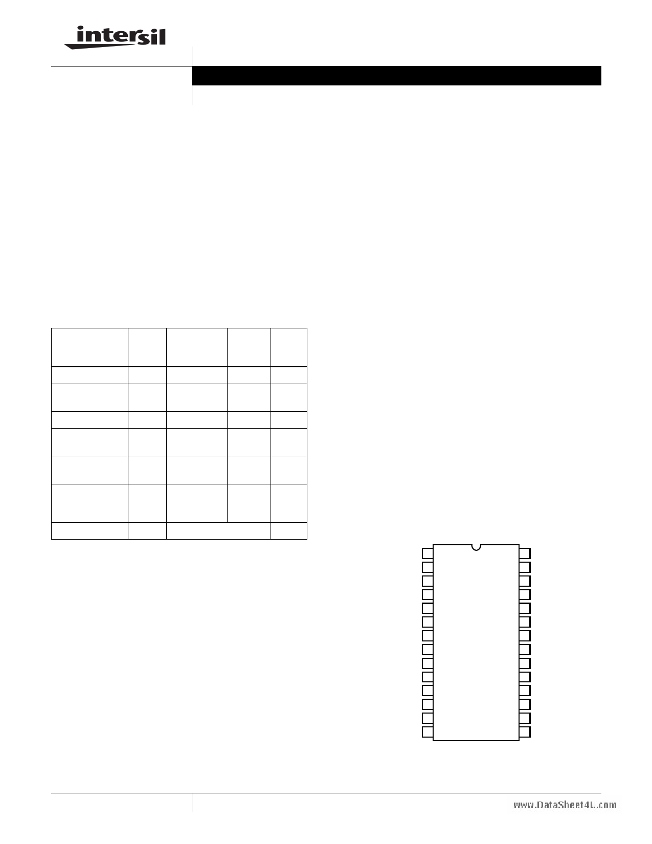
Pinout
HI5960 (SOIC, TSSOP)
TOP VIEW
D13 (MSB) 1
D12 2
D11 3
D10 4
D9 5
D8 6
D7 7
D6 8
D5 9
D4 10
D3 11
D2 12
D1 13
D0 (LSB) 14
28 CLK
27 DVDD
26 DCOM
25 ACOM
24 AVDD
23 COMP2
22 IOUTA
21 IOUTB
20 ACOM
19 COMP1
18 FSADJ
17 REFIO
16 REFLO
15 SLEEP
1 CAUTION: These devices are sensitive to electrostatic discharge; follow proper IC Handling Procedures.
1-888-INTERSIL or 321-724-7143 | Intersil (and design) is a registered trademark of Intersil Americas Inc.
Copyright © Intersil Americas Inc. 2003, 2005. All Rights Reserved. All other trademarks mentioned are the property of their respective owners.
1 page 
HI5960
Electrical Specifications AVDD = DVDD = +5V, VREF = Internal 1.2V, IOUTFS = 20mA, TA = 25oC for All Typical Values (Continued)
PARAMETER
TEST CONDITIONS
MIN TYP MAX UNITS
+5V Power Supply
Total Harmonic Distortion (THD) to
Nyquist
fCLK = 100MSPS, fOUT = 4.0MHz (Notes 4, 8)
fCLK = 50MSPS, fOUT = 2.0MHz (Notes 4, 8)
fCLK = 25MSPS, fOUT = 1.0MHz (Notes 4, 8)
- -71
- -75
- -77
+5V Power Supply
Spurious Free Dynamic Range,
SFDR to Nyquist (fCLK/2)
fCLK = 130MSPS, fOUT = 40.4MHz (Notes 4, 8)
fCLK = 130MSPS, fOUT = 10.1MHz (Notes 4, 8)
fCLK = 130MSPS, fOUT = 5.02MHz, T = 25oC (Notes 4, 8)
- 56
- 67
68 74
fCLK = 130MSPS, fOUT = 5.02MHz, T = Min to Max (Notes 4, 8)
66 -
fCLK = 100MSPS, fOUT = 40.4MHz (Notes 4, 8)
- 55
fCLK = 100MSPS, fOUT = 20.2MHz (Notes 4, 8)
fCLK = 100MSPS, fOUT = 5.04MHz, T = 25oC (Notes 4, 8)
- 63
68 74
fCLK = 100MSPS, fOUT = 5.04MHz, T = Min to Max (Notes 4, 8)
66 -
fCLK = 100MSPS, fOUT = 2.51MHz (Notes 4, 8)
- 76
fCLK = 50MSPS, fOUT = 20.2MHz (Notes 4, 8)
fCLK = 50MSPS, fOUT = 5.02MHz, T = 25oC (Notes 4, 8)
- 65
68 74
fCLK = 50MSPS, fOUT = 5.02MHz, T = Min to Max (Notes 4, 8)
66 -
fCLK = 50MSPS, fOUT = 2.51MHz (Notes 4, 8)
- 77
fCLK = 50MSPS, fOUT = 1.00MHz (Notes 4, 8)
- 79
fCLK = 25MSPS, fOUT = 1.0MHz (Notes 4, 8)
- 79
+5V Power Supply
Multitone Power Ratio
fCLK = 20MSPS, fOUT = 2.0MHz to 2.99MHz, 8 Tones at 110kHz
Spacing (Notes 4, 8)
-
76
-
-
-
-
-
-
-
-
-
-
-
-
-
-
-
-
-
-
dBc
dBc
dBc
dBc
dBc
dBc
dBc
dBc
dBc
dBc
dBc
dBc
dBc
dBc
dBc
dBc
dBc
dBc
dBc
fCLK = 100MSPS, fOUT = 10MHz to 14.95MHz, 8 Tones at 530kHz -
76
-
dBc
Spacing (Notes 4, 8)
+3V Power Supply
Spurious Free Dynamic Range,
SFDR Within a Window
+3V Power Supply
Total Harmonic Distortion (THD) to
Nyquist
fCLK = 100MSPS, fOUT = 20.2MHz, 30MHz Span (Notes 4, 8)
fCLK = 100MSPS, fOUT = 5.04MHz, 8MHz Span (Notes 4, 8)
fCLK = 50MSPS, fOUT = 5.02MHz, 8MHz Span (Notes 4, 8)
fCLK = 100MSPS, fOUT = 4.0MHz (Notes 4, 8)
fCLK = 50MSPS, fOUT = 2.0MHz (Notes 4, 8)
fCLK = 25MSPS, fOUT = 1.0MHz (Notes 4, 8)
- 80
- 95
- 95
- -70
- -74
- -76
-
-
-
-
-
-
dBc
dBc
dBc
dBc
dBc
dBc
5
5 Page 
HI5960
Small Outline Plastic Packages (SOIC)
N
INDEX
AREA
E
-B-
H
0.25(0.010) M B M
123
-A-
D
SEATING PLANE
A
L
h x 45o
-C-
e A1
B
0.25(0.010) M C A M B S
α
0.10(0.004)
C
NOTES:
1. Symbols are defined in the “MO Series Symbol List” in Section 2.2
of Publication Number 95.
2. Dimensioning and tolerancing per ANSI Y14.5M-1982.
3. Dimension “D” does not include mold flash, protrusions or gate
burrs. Mold flash, protrusion and gate burrs shall not exceed
0.15mm (0.006 inch) per side.
4. Dimension “E” does not include interlead flash or protrusions. In-
terlead flash and protrusions shall not exceed 0.25mm (0.010
inch) per side.
5. The chamfer on the body is optional. If it is not present, a visual
index feature must be located within the crosshatched area.
6. “L” is the length of terminal for soldering to a substrate.
7. “N” is the number of terminal positions.
8. Terminal numbers are shown for reference only.
9. The lead width “B”, as measured 0.36mm (0.014 inch) or greater
above the seating plane, shall not exceed a maximum value of
0.61mm (0.024 inch)
10. Controlling dimension: MILLIMETER. Converted inch dimen-
sions are not necessarily exact.
M28.3 (JEDEC MS-013-AE ISSUE C)
28 LEAD WIDE BODY SMALL OUTLINE PLASTIC PACKAGE
INCHES
MILLIMETERS
SYMBOL MIN MAX MIN MAX NOTES
A
0.0926 0.1043 2.35
2.65
-
A1
0.0040 0.0118 0.10
0.30
-
B
0.013 0.0200 0.33
0.51
9
C
0.0091 0.0125 0.23
0.32
-
D 0.6969 0.7125 17.70 18.10
3
E
0.2914 0.2992 7.40
7.60
4
e 0.05 BSC
1.27 BSC
-
H 0.394 0.419 10.00 10.65
-
h 0.01 0.029 0.25 0.75 5
L
0.016 0.050 0.40
1.27
6
N 28
28 7
α 0o 8o 0o 8o -
Rev. 0 12/93
11
11 Page | ||
| Páginas | Total 12 Páginas | |
| PDF Descargar | [ Datasheet HI5960.PDF ] | |
Hoja de datos destacado
| Número de pieza | Descripción | Fabricantes |
| HI5960 | High Speed D/A Converter | Intersil Corporation |
| Número de pieza | Descripción | Fabricantes |
| SLA6805M | High Voltage 3 phase Motor Driver IC. |
Sanken |
| SDC1742 | 12- and 14-Bit Hybrid Synchro / Resolver-to-Digital Converters. |
Analog Devices |
|
DataSheet.es es una pagina web que funciona como un repositorio de manuales o hoja de datos de muchos de los productos más populares, |
| DataSheet.es | 2020 | Privacy Policy | Contacto | Buscar |