|
|
|
PDF HI20206 Data sheet ( Hoja de datos )
| Número de pieza | HI20206 | |
| Descripción | 3-Channel D/A Converter | |
| Fabricantes | Intersil Corporation | |
| Logotipo | ||
Hay una vista previa y un enlace de descarga de HI20206 (archivo pdf) en la parte inferior de esta página. Total 13 Páginas | ||
|
No Preview Available !
August
Semiconductor
1997
NOT
RECOMMENSDeEe DHIF1O17R8NEW
DESIGNS
HI20206
Triple 8-Bit, 35 MSPS, RGB,
3-Channel D/A Converter
Features
Description
• Resolution . . . . . . . . . . . . . . . . . . . . . . . . . . . Triple 8-Bit
• Maximum Conversion Speed . . . . . . . . . . . . . . . 35MHz
• RGB 3-Channel Input/Output
• Differential Linearity Error . . . . . . . . . . . . . . . ±1/2 LSB
• Digital Input Voltage . . . . . . . . . . . . . . . . . . . .TTL Level
• Output Voltage Full-Scale . . . . . . . . . . . . . . 1VP-P (Typ)
• Low Power Consumption . . . . . . . . . . . . . 360mW (Typ)
• +5V Single Power Supply
The HI20206 is a triple 8-bit, high-speed, bipolar D/A
converter designed for video band use. It has three sepa-
rate, 8-bit pixel inputs, one each for red, green, and blue
video data. A single 5.0V power supply and pixel clock input
is all that is required to make the device operational. A bias
voltage generator is internal. For lower CMOS power
consumption, refer to the HI1178.
Ordering Information
• Direct Replacement for Sony CX20206
Applications
• Digital TV
TEMP.
PART NUMBER RANGE (oC) PACKAGE
PKG. NO.
HI20206JCP
-20 to 75 42 Ld PDIP E42.6B-S
• Graphics Display
• High Resolution Color Graphics
• Video Reconstruction
• Instrumentation
• Image Processing
• I/Q Modulation
www.DataSheet4U.com
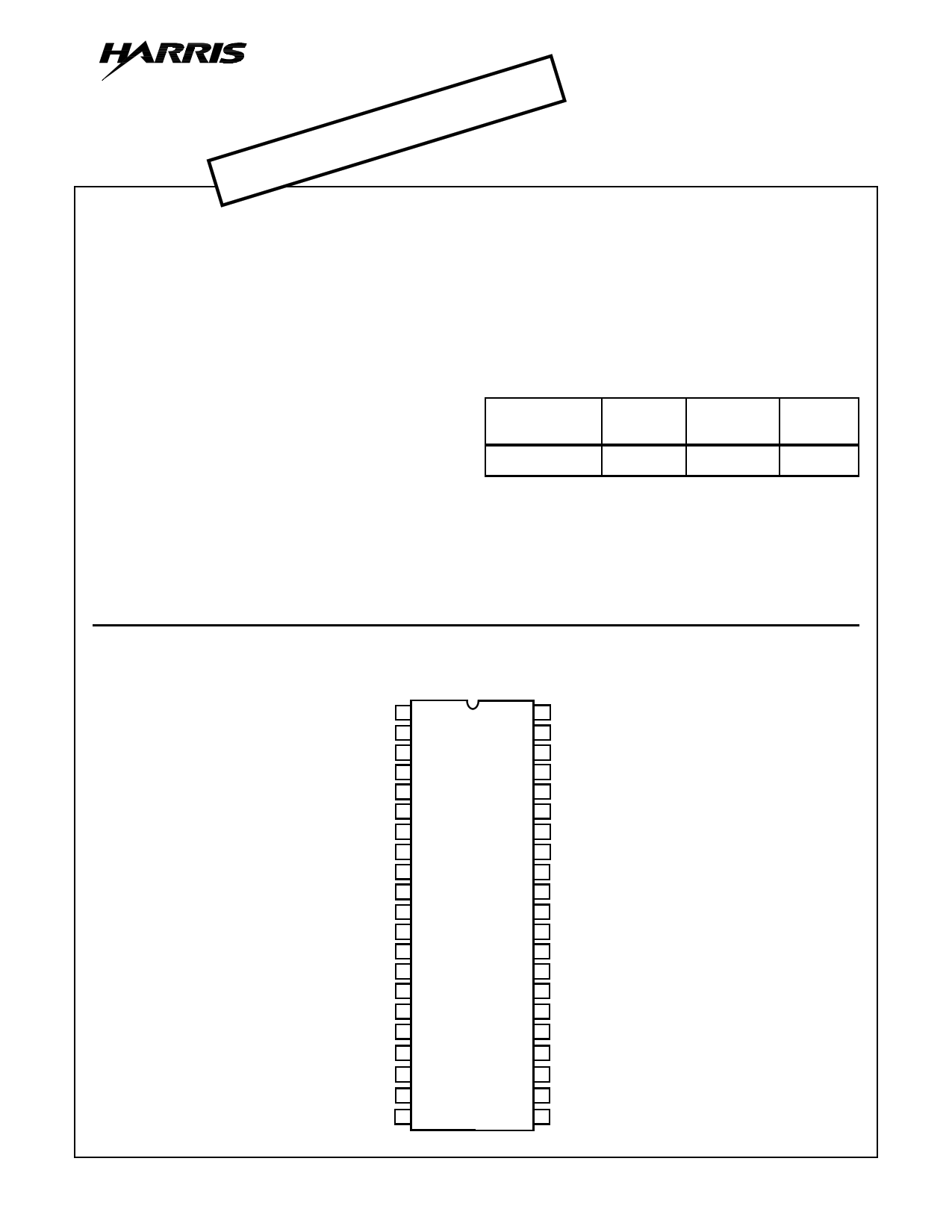
Pinout
HI20206 (PDIP)
TOP VIEW
R5 1
R6 2
R7 3
R8 4
G1 5
G2 6
G3 7
G4 8
G5 9
G6 10
G7 11
G8 12
B1 13
B2 14
B3 15
B4 16
B5 17
B6 18
B7 19
B8 20
CLK 21
42 R4
41 R3
40 R2
39 R1
38 NC
37 DGND
36 NC
35 ROUT
34 NC
33 GOUT
32 NC
31 BOUT
30 NC
29 AVCC
28 NC
27 VSET
26 VREF
25 AGND
24 NC
23 NC
22 DVCC
CAUTION: These devices are sensitive to electrostatic discharge. Users should follow proper IC Handling Procedures.
Copyright © Harris Corporation 1997
10-1
File Number 4111.1
1 page 
HI20206
Absolute Maximum Ratings
Supply Voltage (VCC) . . . . . . . . . . . . . . . . . . . . . . . . . . . . . .0V to 7V
Input Voltage (Digital) (VI, VCLK) . . . . . . . . . . . . . . . . . -0.3V to VCC
Output Voltage (Analog) (VSET) . . . . . . . . . . . . . . VCC -2.1V to VCC
Output Current
Analog (IOUT) . . . . . . . . . . . . . . . . . . . . . . . . . . . . . -3mA to 10mA
VREF Pin (IREF) . . . . . . . . . . . . . . . . . . . . . . . . . . . . -5mA to 0mA
Supply Voltage Range (Typ) . . . . . . . . . . . . . . . . . . . . . . . 5V to 10V
Thermal Information
Thermal Resistance (Typical, Note 2)
θJA (oC/W)
PDIP Package . . . . . . . . . . . . . . . . . . . . . . . . . . . . .
70
Maximum Storage Temperature Range (TSTG) . . . .-65oC to 150oC
Maximum Lead Temperature (Soldering 10s) . . . . . . . . . . . . . 300oC
Recommended Operating Conditions
Supply Voltage
AVCC, DVCC . . . . . . . . . . . . . . . . . . . . . . . . . . . . . . . .4.5V to 5.5V
AVCC-DVCC . . . . . . . . . . . . . . . . . . . . . . . . . . . . . . . -0.2V to 0.2V
AGND-DGND . . . . . . . . . . . . . . . . . . . . . . . . . . . . -0.05V to 0.05V
Digital Input Voltage
H Level (VIH, VCLKH) . . . . . . . . . . . . . . . . . . . . . . . .2.0V to DVCC
L Level (VIL, VCLKL) . . . . . . . . . . . . . . . . . . . . . . . . DGND to 0.8V
VSET Input Voltage (VSET). . . . . . . . . . . . . . . . . . . . . . .0.7V to 0.9V
VREF Pin Current (IREF). . . . . . . . . . . . . . . . . . . . . . -3mA to -0.4mA
Clock Pulse Width
tPW1 . . . . . . . . . . . . . . . . . . . . . . . . . . . . . . . . . . . . . . . . . . . .15ns
tPW0 . . . .
Temperature
......
Range
......
(TOPR)
.
.
.
.
.
.
.
.
.
.
.
.
.
.
.
.
.
.
.
.
.
.
.
.
.
.
.
.
.
.
.
.
.
.
.
.
.
.
.
.
.....
-40oC
..
to
.10ns
85oC
CAUTION: Stresses above those listed in “Absolute Maximum Ratings” may cause permanent damage to the device. This is a stress only rating and operation
of the device at these or any other conditions above those indicated in the operational sections of this specification is not implied.
NOTE:
2. θJA is measured with the component mounted on an evaluation PC board in free air.
Electrical Specifications
PARAMETER
Resolution
Monotonic
Differential Linearity Error
Integral Linearity Error
TA = 25oC, AVCC = DVCC = 5V, AGND = DGND = 0V
SYMBOL
TEST
CONDITIONS
RSL
MNT
DLE
ILE
VSET - AGND = 0.8V,
RL > 10kΩ
MIN
-
-
-0.5
-0.4
Maximum Conversion Speed
Full Scale Output Voltage (Note 3)
RGB Output Voltage Full Scale Ratio (Note 4)
Output Zero Offset Voltage
Output Resistance
Dissipation Current
Digital Data Input
Current
H Level
L Level
Clock Input Current
VSET Input Current
Internal Reference Voltage
Set-Up Time
Hold Time
Crosstalk Among R, G and B
Upper 2 Bits
Lower 6 Bits
Upper 2 Bits
Lower 6 Bits
H Level
L Level
fMAX
VOFS
FSR
VOFFSET
RO
ID
IIH(U)
IIH(L)
IIL(U)
IIL(U)
ICLKH
ICLKL
ISET
VREF
tS
tH
CT
VSET - AGND = 0.8V,
RL > 10kΩ, CL < 20pF
VSET - AGND = 0.8V,
RL > 10kΩ, IREF = -400µA
VI = DVCC
VI = DGND
VCLK = DVCC
VCLK = DGND
VSET - AGND = 0.8V
IREF = -400µA
D/A OUT: 1VP-P, RL>10kΩ,
CL<20pF, fDATA = 7MHz,
fCLK = 14MHz, See Figure 5
35
0.85
0
-40
270
54
-
-
-10
-10
-
-10
-5
1.08
12
3
-
TYP
8
Guarantee
-
-
-
1.0
4
-6
340
72
1.2
0.6
0
0
3
0
-0.3
1.20
-
-
-40
MAX
-
-
0.5
0.4
-
1.15
8
0
420
90
20
10
10
10
30
10
0
1.32
-
-
-33
UNITS
Bit
-
LSB
% of Full
Scale
MHz
VP-P
%
mV
Ω
mA
µA
µA
µA
µA
µA
µA
µA
V
ns
ns
dB
10-5
5 Page 
HI20206
(2) Phase Relationship Between Data and Clock
In order to obtain the desired characteristics as a D/A
converter, it is necessary to set the phase relationship
correctly between the externally applied data and
clock.
Satisfy the standard of the set-up time (tS) and hold
time (tH) indicated in the electrical characteristics. As to
the meaning of tS and tH, see the timing chart.
Moreover, the clock pulse width is desired to be as
indicated in the recommended operating condition.
(3) Regarding the Load of D/A Output Pin
Receive the D/A output of the next stage with high
impedance. In other words perform so that it becomes
as follows:
RL > 10kΩ
CL < 20pF.
The temperature characteristics indicated in the
characteristics diagram has been measured under this
condition.
However, when it is made RL ≤ 10kΩ the temperature
characteristics may change considerably. In addition,
when it is made to CL ≥ 20pF, the rise and fall of the
D/A output become slow and will not operate at high
speed.
(4) Noise Reduction Measures
As the D/A output voltage is a minute voltage of
approximately 4mV per one step, ingenuity is required
in reducing the noise entering from the outside of the
IC as much as possible. Therefore, use the items given
below as reference.
• When mounting onto the printed board, allow as
much space as possible to the ground surface and
the VCC surface on the board and reduce the para-
sitic inductance and resistance.
• It is desirable that the AGND and DGND be sepa-
rated in the pattern on the board. It is similar with
AVCC and DVCC. As shown in the diagram below, for
example, it is recommended that the wiring to the
electric supply of AGND and DGND as also AVCC
and DVCC be conducted separately, and then mak-
ing AGND and DGND as also AVCC and DVCC in
common right near the power supply respectively.
• Insert in parallel a 47µF tantalum capacitor and a
100pF ceramic capacitor between the VCC surface
on the printed board and the nearmost ground sur-
face. (A of diagram below). It is also desirable to
insert the above between the VCC surface near the
pin of the IC and the ground surface (see Figure 11).
They are bypass capacitors to prevent bad effects
from occurring to the characteristics when the power
supply voltage fluctuates due to the clock, etc.
It is recommended to reduce noise which overlaps
the D/A output by inserting a capacitor of over 0.1µF
between pin 25 (AGND) and pin 26 (VSET).
HI20206
A
PRINTED BOARD
DGND
DVCC
AVCC
AGND
B
POWER SUPPLY
FIGURE 11.
10-11
11 Page | ||
| Páginas | Total 13 Páginas | |
| PDF Descargar | [ Datasheet HI20206.PDF ] | |
Hoja de datos destacado
| Número de pieza | Descripción | Fabricantes |
| HI20201 | 10-Bit Ultra High Speed D/A Converter | Intersil |
| HI20203 | Ultra High-Speed D/A Converter | Intersil Corporation |
| HI20206 | 3-Channel D/A Converter | Intersil Corporation |
| Número de pieza | Descripción | Fabricantes |
| SLA6805M | High Voltage 3 phase Motor Driver IC. |
Sanken |
| SDC1742 | 12- and 14-Bit Hybrid Synchro / Resolver-to-Digital Converters. |
Analog Devices |
|
DataSheet.es es una pagina web que funciona como un repositorio de manuales o hoja de datos de muchos de los productos más populares, |
| DataSheet.es | 2020 | Privacy Policy | Contacto | Buscar |