|
|
|
PDF EM6607 Data sheet ( Hoja de datos )
| Número de pieza | EM6607 | |
| Descripción | Ultra-low power microcontroller | |
| Fabricantes | EM Microelectronic | |
| Logotipo | ||
Hay una vista previa y un enlace de descarga de EM6607 (archivo pdf) en la parte inferior de esta página. Total 30 Páginas | ||
|
No Preview Available !
R
EM MICROELECTRONIC - MARIN SA
EM6607
Ultra-low power microcontroller
with 4 high drive outputs
Features
Low Power typical 1.8µA active mode
typical 0.5µA standby mode
typical 0.1µA sleep mode
@ 1.5V, 32kHz, 25 °C
Low Voltage 1.2 to 3.3 V
ROM
2k × 16 (Mask Programmed)
RAM
96 × 4 (User Read/Write)
2 clocks per instruction cycle
RISC architecture
5 software configurable 4-bit ports
1 High drive output port
Up to 20 inputs
(5 ports)
Up to 16 outputs
(4 ports)
buzzer three tone
Serial Write buffer – SWB
Supply Voltage level detection (SVLD).
Analogue and timer watchdog
8 bit timer / event counter
Internal interrupt sources (timer, event counter,
prescaler)
External interrupt sources (portA + portC)
Description
The EM6607 is a single chip low power, mask
programmed CMOS 4-bit microcontroller. It contains
ROM, RAM, watchdog timer, oscillation detection circuit,
combined timer / event counter, prescaler, voltage level
detector and a number of clock functions. Its low voltage
and low power operation make it the most suitable
controller for battery, stand alone and mobile equipment.
The EM6607 microcontroller is manufactured using EM’s
Advanced Low Power CMOS Process.
In 24 Pin package it is direct replacement for EM6603.
Typical Applications
sensor interfaces
domestic appliances
clocks
security systems
bicycle computers
automotive controls
TV & audio remote controls
measurement equipment
R/F and IR. control
motor driving
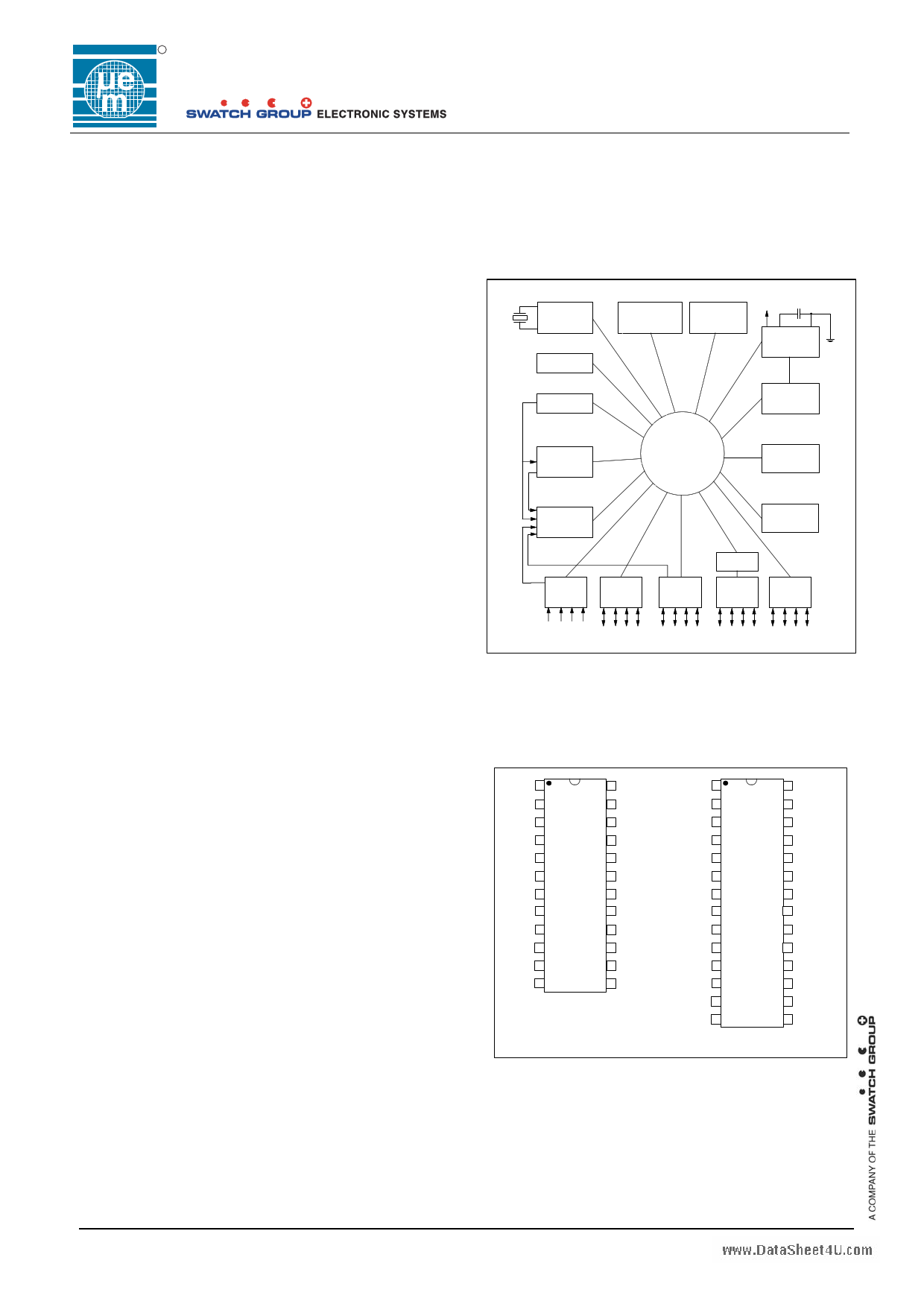
Figure 1. Architecture
32KHz
Crystal Osc
VLD 3 Levels
Prescaler
ROM
2k X 16Bit
RAM
96 X 4Bit
V VDD REG
V SS
Power
Supply
Power on
Reset
8-Bit Event
Count/Timer
Core
EM6600
3 Tone
Buzzer
Interrupt
Controller
Watchdog
Timer
Port A
0 123
Port B
0 123
Port C
0 123
Serial Write
Buffer
Port D
Port E
0123 0 123
High Drive
Outputs
Clk Buzzer
Data
Figure 2. Pin Configuration
PA0 1
24 VDD
PA1 2
23 VREG
PA2 3
22 RESET
PA3 4
21 PD3
PB0 5
20 PD2
PB1
PB2
6
7
EM6607
19 PD1
18 PD0
PB3 8
17 PC3
TEST 9
16 PC2
QOUT 10
15 PC1
QIN11
14 PC0
VSS12
13 STB/RST
PA0 1
28 VDD
PA1 2
27 VREG
PA2 3
26 RESET
PA3 4
25 PE3
PE0 5
24 PD3
PB0 6
23 PD2
PB1 7 EM6607 22 PD1
PB2 8
21 PD0
PB3 9
20 PE2
PE1 10
19 PC3
TEST 11 EM6680 18 PC2
QOUT 12
17 PC1
QIN 13
16 PC0
VSS 14
15 STB/RST
(TS)SOP-24
(TS)SOP-28
Copyright © 2005, EM Microelectronic-Marin SA
1
www.emmicroelectronic.com
1 page 
R
1 Pin Description for EM6607
Pin Nb
24 pin
1
2
3
4
-
5
6
7
8
-
9
10
11
12
13
14
15
16
17
-
18
19
20
21
-
22
23
24
Table 1.
Pin Nb Pin Name
28 pin
1 port A, 0
2 port A, 1
3 port A, 2
4 port A, 3
5 port E, 0
6 port B, 0
7 port B, 1
8 port B, 2
9 port B, 3
10 port E, 1
11 test
12 Qout/osc 1
13 Qin/osc 2
14 VSS
15 STB/RST
16 port C, 0
17 port C, 1
18 port C, 2
19 port C, 3
20 port E, 2
21 port D, 0
22 port D, 1
23 port D, 2
24 port D, 3
25 port E, 3
26 RESET
27 VREG
28 VDD
Pin Description
Function
input 0 port A
input 1 port A
input 2 port A
input 3 port A
input / output 0 port E
input / output 0 port B
input / output 1 port B
input / output 2 port B
input / output 3 port B
input / output 1 port E
test input terminal
crystal terminal 1
crystal terminal 2 (input)
negative power supply terminal
strobe / reset status
input / output 0 port C
input / output 1 port C
input / output 2 port C
input / output 3 port C
input / output 2 port E
input / output 0 port D
input / output 1 port D
input / output 2 port D
input / output 3 port D
input / output 3 port E
reset terminal
internal voltage regulator
positive power supply terminal
EM6607
Remarks
interrupt request; tvar 1
interrupt request; tvar 2
interrupt request; tvar 3
interrupt request; event counter input
buzzer output in 28 pin package
buzzer output in 24 pin package
for EM test purpose only (internal pull-down)
Can accept trimming capacitor tw. VSS
µC reset state + port B, C, D write
interrupt request
interrupt request
interrupt request
interrupt request
SWB Serial Clock Output
SWB Serial Data Output
Active high (internal pull-down)
Needs typ. 100nF capacitor tw. VSS
Copyright © 2005, EM Microelectronic-Marin SA
5
www.emmicroelectronic.com
5 Page 
R
4.6 CPU State after RESET
RESET initialises the CPU as shown in the table below.
Table 7. Initial Value after RESET
name
Program counter 0
Program counter 1
Program counter 2
stack pointer
index register
Carry flag
Zero flag
HALT
Instruction register
periphery registers
bits
12
12
12
2
7
1
1
1
16
4
symbol
PC0
PC1
PC2
SP
IX
CY
Z
HALT
IR
initial value
$000 (as a result of Jump 0)
undefined
undefined
SP(0) selected
undefined
undefined
undefined
0
Jump 0
see peripheral memory map
EM6607
4.7 POR with Power-Check Reset
POR and Power-Check are
guarantee proper operation
supervising the
after Power-On.
VREG
The
(digital) which follows more or less
resetcold signal is released when
the
the
VDD
V
supply
supply
voltage
voltage
on start-up to
is high enough
for the IC to function correctly.
DD
During power-up of the EM6607 static POR (Power-On-Reset) cell supervising the VREG with level of typ. 0.9V is checked to
give initial reset. Reset can be prolonged also with Power-Check function if enabled by metal option. In this case VDD must
come
above
VL1
of
the
SVLD
described
in
Chapter
11
13H
Supply
134H
Voltage
Level
Detector
(SVLD)
to release the circuit reset
signal and starts to execute instructions.
When Power-Check is enabled a power-check logic is switched-on with POR signal high and starts to check periodically
VDD against the SVLD-VL1 level which keeps resetcold active high until VDD > VL1. When used with external quartz first VDD
check starts in the middle of quartz Cold-Start sequence – after first 16384 system clocks with the same timing as in normal
SVLD operation. If VDD > VL1 Power-Check condition is met and system reset will wait until first 32768 clocks needed for
Quartz Cold-Start is finished and release System reset.
In case VDD < VL1, comparison will be repeated with every next 8 Hz system clock until VDD > VL1. In case of a very slow
rising VDD, it might happen that Quartz Cold-Start is finished. System reset will keep the EM6607 under reset until first time
VDD becomes higher as VL1 to guarantee good operating conditions (oscillator stabilized during its Cold-Start delay and VDD
is high enough to avoid “grey” zone between static POR and VL1).
IMPORTANT: special care should be taken, when Power Supply starts to fall close to or below V min. Frequent checking
DD
of
the
SVLD
VL1
(1.3V)
must
be
done.
Between
minimum
V
DD
supply
of
1.2V
and
static
POR
level
of
0.9V
there
is
a
grey
zone, which must be avoided for proper operation.
Copyright © 2005, EM Microelectronic-Marin SA
11
www.emmicroelectronic.com
11 Page | ||
| Páginas | Total 30 Páginas | |
| PDF Descargar | [ Datasheet EM6607.PDF ] | |
Hoja de datos destacado
| Número de pieza | Descripción | Fabricantes |
| EM6603 | Ultra Low Power Multi I/O Microcontroller | EM Microelectronic |
| EM6604 | Ultra Low Power Multi I/O Microcontroller | EM Microelectronic |
| EM6605 | 4 bit Microcontroller | EM Microelectronic |
| EM6607 | Ultra-low power microcontroller | EM Microelectronic |
| Número de pieza | Descripción | Fabricantes |
| SLA6805M | High Voltage 3 phase Motor Driver IC. |
Sanken |
| SDC1742 | 12- and 14-Bit Hybrid Synchro / Resolver-to-Digital Converters. |
Analog Devices |
|
DataSheet.es es una pagina web que funciona como un repositorio de manuales o hoja de datos de muchos de los productos más populares, |
| DataSheet.es | 2020 | Privacy Policy | Contacto | Buscar |