|
|
|
PDF FSA201 Data sheet ( Hoja de datos )
| Número de pieza | FSA201 | |
| Descripción | USB2.0 Full-Speed and Audio Switches | |
| Fabricantes | Fairchild Semiconductor | |
| Logotipo | ||
Hay una vista previa y un enlace de descarga de FSA201 (archivo pdf) en la parte inferior de esta página. Total 19 Páginas | ||
|
No Preview Available !
Click to see this datasheet
in Simplified Chinese!
January 2007
FSA201 USB2.0 Full-Speed and Audio Switches
with Negative Signal Capability
Features
3Ω Typical ON Resistance
-3db Bandwidth: > 250MHz
Low Power Consumption
Packaged in Pb-free 10-Lead MicroPak™
(1.6 x 2.1mm), 10-pin MSOP (Preliminary)
Power-off Protection on Common D+/R, D-/L Ports
Automatically Detects Vbus for Switch Path
Selection
Applications
Cell Phone, PDA, Digital Camera, and Notebook
LCD Monitor, TV, and Set-top Box
Description
The FSA201 is a Double-Pole, Double Throw (DPDT)
multiplexer that combines a low-distortion audio and a
USB2.0 Full-Speed (FS) switch path. This configuration
enables audio and USB data to share a common
connector port. The architecture is designed to allow
audio signals to swing below ground. This means a common
USB and headphone jack can be used for personal media
players and similar portable peripheral devices.
Since USB2.0 is an industry standard for shared data-
path in portable devices, the FSA201 also incorporates
a Vbus detection capability. The FSA201 includes a
power-off feature to minimize current consumption when
Vbus is not present. This power-off circuitry is available
for the common D+/R, D-/L ports only. Typical
applications involve switching in portables and
consumer applications, such as cell phones, digital
cameras, and notebooks with hubs or controllers.
www.DataSheet4U.com
Ordering Information
Part Number
FSA201L10X
FSA201MUX (Preliminary)
Package Number Pb-Free
MAC010A
Yes
MUA10A
Yes
Packing Description
10-Lead MicroPak, JEDEC MO-255, 1.6 x 2.1mm
10-Lead MSOP JEDEC MO-187, 3.0 mm Wide
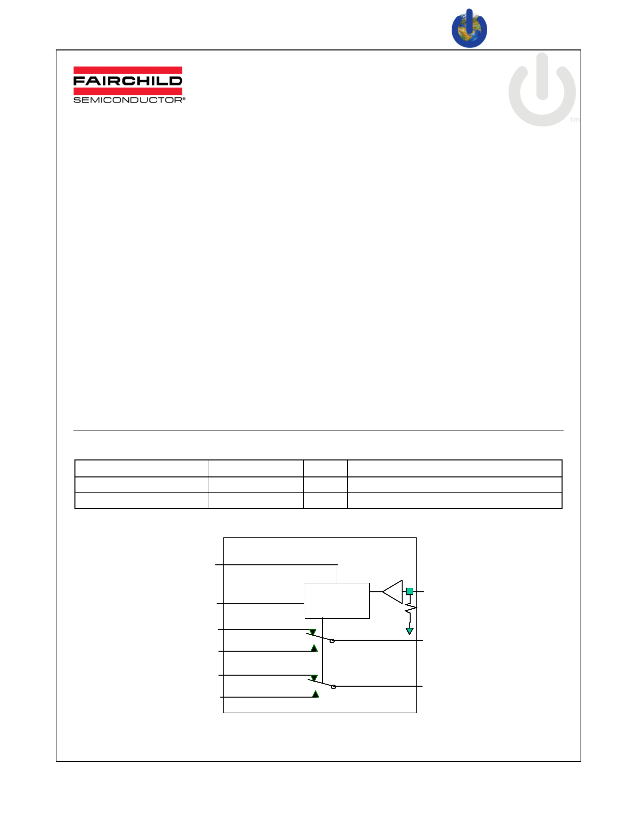
Vbus
Vaudio
D+
R
Switch Select
Control Circuitry
ASel
Rpd
GND
D+/R
D- D-/L
L
Figure 1. FSA201 Analog Symbol
© 2006 Fairchild Semiconductor Corporation
FSA201 Rev. 1.1.9
www.fairchildsemi.com
1 page 
DC Electrical Characteristics
All typical values are at 25ºC unless otherwise specified.
Symbol
Parameter
VAudio
(V)
Conditions
TA = - 40ºC to +85ºC Unit
Min. Typ. Max.
Common Pins
VIK
Clamp Diode
Voltage
2.7 IIK = -18mA
-1.2
VIH
Control Input
Voltage HIGH
2.7 to 3.6
1.3 V
VIL
Control Input
Voltage LOW
2.7 to 3.6
0.5
IIN
ASel Input HIGH
Current
3.6 VCNTRL = 0V to 3.6V
-3 3 µA
Power Off Leakage
IOFF
Current (Common
Port Only D+/R, D-
Vaudio = Common Port (D+/R, D-/L)
Vbus = 0V VSW = 0V to 5.5V
/L)
1 µA
INO(0FF)
Off-
LeakageCurrent of
Port
D+, D-, R, L
Vbus = 0V, 5. 5V
D+/R, D-/L = 0.3V, VAUDIO – 0.3V
3.6
D+, D-, R, L = 0.3V, VAUDIO –0.3V
-50
10
50
nA
or Floating
See Figure 14
INC(0N)
On-
LeakageCurrent of
Port D+/R or D-/L
Vbus = 0V, 5.5V
3.6
D+/R, D-/L = 0.3V, VAUDIO – 0.3V
D+, D-, R, L = Floating
-100
50
100
nA
See Figure 15
USB Switch Path
USB Analog Signal
Range
Vbus (V)
0 3.6 V
RONUSB
∆ RONUSB
FS Switch On
Resistance(4)
FS Delta RON(4,6)
4.25
4.25
VD+/D- = 0V, 3.0V, ION = -8mA
See Figures 6, 13
VD+/D- = 3V, ION = -8mA
36
0.35
Ω
Ω
Audio Switch Path
Audio Analog
Signal Range
VAudio (V)
Vaudio –
6.5
Vaudio
V
RONAudio
Audio Switch On
Resistance(7)
∆ RONAudio
RFLAT(Audio)
Audio Delta RON(4)
Audio RON
Flatness(5)
VL/R = -2V, 0V, 0.7V, VAUDIO-0.7V,
2.7 VAUDIO ION = -100mA, Vbus = 0V
See Figures 5, 13
2.7 VL/R = 0.7V ION = -100mA
2.7
VL/R = -2V, 0V, 0.7V, 2V, 2.7V
ION = -100mA
0.5 1.0
0.01 0.1
0.35
Ω
Ω
Ω
Notes:
4. ∆ RON=RON max – RON min measured at identical VCC, temperature, and voltage. Worst-case signal path, audio or
USB channel, is characterized.
5. Flatness is defined as the difference between the maximum and minimum values of on resistance over the
specified range of conditions.
6. Guaranteed by characterization, not production tested.
7. On resistance is determined by the voltage drop between the A and B pins at the indicated current through the switch.
© 2006 Fairchild Semiconductor Corporation
FSA201 Rev. 1.1.9
5
www.fairchildsemi.com
5 Page 
Typical Characteristics (Continued)
1
0
-10
-20
-30
-40
-50
-60
-70
-80
-90
-100
10 100 1000
Frequency (MHz)
Figure 9. Non-Adjacent Channel Crosstalk (Audio) Characterization at VCC (VAUDIO) = 2.7V
Figure 10. Non-Adjacent Channel Crosstalk (USB) Characterization at VCC (Vbus) = 4.25V
© 2006 Fairchild Semiconductor Corporation
FSA201 Rev. 1.1.9
11
www.fairchildsemi.com
11 Page | ||
| Páginas | Total 19 Páginas | |
| PDF Descargar | [ Datasheet FSA201.PDF ] | |
Hoja de datos destacado
| Número de pieza | Descripción | Fabricantes |
| FSA2002 | Diode ( Rectifier ) | American Microsemiconductor |
| FSA2002M | Diode ( Rectifier ) | American Microsemiconductor |
| FSA2003 | Diode ( Rectifier ) | American Microsemiconductor |
| FSA2003M | Diode ( Rectifier ) | American Microsemiconductor |
| Número de pieza | Descripción | Fabricantes |
| SLA6805M | High Voltage 3 phase Motor Driver IC. |
Sanken |
| SDC1742 | 12- and 14-Bit Hybrid Synchro / Resolver-to-Digital Converters. |
Analog Devices |
|
DataSheet.es es una pagina web que funciona como un repositorio de manuales o hoja de datos de muchos de los productos más populares, |
| DataSheet.es | 2020 | Privacy Policy | Contacto | Buscar |