|
|
|
PDF AAT8640 Data sheet ( Hoja de datos )
| Número de pieza | AAT8640 | |
| Descripción | ONE-CELL LI-ION BATTERY PROTECTION IC | |
| Fabricantes | AAT | |
| Logotipo | ||
Hay una vista previa y un enlace de descarga de AAT8640 (archivo pdf) en la parte inferior de esta página. Total 25 Páginas | ||
|
No Preview Available !
Advanced Analog Technology, Inc.
AAT8640 Series
Product information presented is current as of publication date. Details are subject to change without notice.
ONE-CELL LI-ION BATTERY PROTECTION IC
FEATURES
GENERAL DESCRIPTION
z Ideal for One-Cell Rechargeable Li-Ion
Battery Packs
z High Accuracy Voltage Detection
z Low Current Consumption:
3μA Supply Current (Typical)
The AAT8640 series are designed to protect
one-cell rechargeable Li-Ion battery pack against
over-charge, over-discharge, over-current and
short circuit. They use CMOS process to provide
high accuracy voltage detection and low current
0.1μA Shutdown Current
z 3-Level Over Current Detection:
Over-Current Level 1 /Over Current Level 2
/ Short Circuit
consumption.
Each of the AAT8640 devices incorporates
voltage comparators, bandgap reference voltage
generator, signal delay circuit, short circuit
z Wide Operating Temperature
− 40οC to 85οC
z Small SOT25 Package
Range: detector, and digital control circuit.
In the charge process, when the battery voltage is
www.DataSheet4U.com
charged to a value greater than VC1(Over-Charge
Threshold Voltage), the output of Cout pin
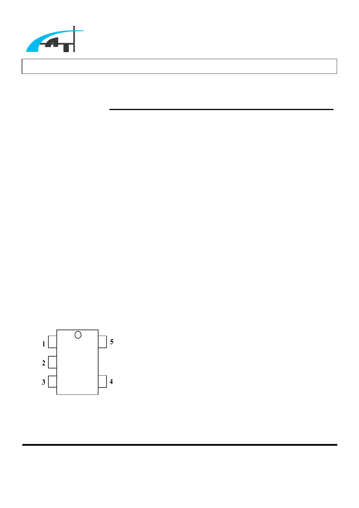
PIN CONFIGURATION
TOP VIEW
switches to the low level, i.e., the VN pin level.
The output of Cout pin will switch to high level
when the battery voltage falls lower than VC2
(Over-Charge Release Voltage), or when the
charger is disconnected from the battery pack and
VN
VDD
GND
COUT
DOUT
the battery voltage level ranges between VC1 and
VC2.
During the discharge process, when the battery
voltage drops to a value lower than VD1
(Over-Discharge Threshold Voltage), the output
of Dout pin switches to low level immediately
(SOT25)
after the internal delay time elapses. The output
of Dout pin will switch to high level when the
battery voltage is at a level higher than VD2
(Over-Discharge Release Voltage).
– 台灣類比科技股份有限公司 –
– Advanced Analog Technology, Inc. –
Page 1 of 25
V2.0
1 page 
Advanced Analog Technology, Inc.
AAT8640 Series
AAT8640B DETECTION VOLTAGE AND DELAY TIME (25℃)
PARAMETER
SYMBOL TEST CONDITION
Over Charge Threshold Voltage
VC1
Detect Rising Edge of Supply
Voltage
Over Charge Release Voltage
VC2
Detect Falling Edge of Supply
Voltage
Over Discharge Threshold
Voltage
VD1
Detect Falling Edge of Supply
Voltage
Over Discharge Release Voltage
VD2
Detect Rising Edge of Supply
Voltage
Over Charge Delay Time
t C1 VDD = 3.6V to 4.5V
Over Discharge Delay Time
t D1 VDD = 3.6V to 2.2V
Over Current Level 1 Detection
Voltage
VOC1
Detect Rising Edge of “VN” Pin
Voltage ( D out Response with tOC1
Delay Time)
Over Current Level 2 Detection
Voltage
VOC2
Detect Rising Edge of “VN”
Pin Voltage ( Dout Response
with tOC2 Delay Time)
VDD = 3.0V , Detect Rising Edge
Short Circuit Detection Voltage
Vshort
of “VN” Pin Voltage ( D out
Response with t short Delay
Time)
Over Current Level 1 Detection
Delay Time
t OC1
VDD = 3.0V
Room Temp. ⇒
Over Current Level 2 Detection
Delay Time
t OC2
Low or High Temp. ⇒
VDD = 3.0V
Short Circuit Detection Delay
Time
t short
VDD = 3.0V
Charger Detection Voltage
VCHR
Detect Rising Edge of “ Dout ”
Pin Voltage
(when VD1<VDD<VD2)
C out High Level Resistance
R COH
VDD = 3.5V ; C OUT = 3.0V ;
VN = 0V
C out Low Level Resistance
R COL
VDD = 4.5V ;
COUT = 0.5V ; VN = 0V
Dout High Level Resistance
R DOH
VDD = 3.5V ; D out = 3.0V ;
VN = 0V
D out Low Level Resistance
R DOL
VDD = 1.8V ;
D out = 0.5V ; VN = 1.8V
Internal Resistance between VN
and VDD
R VND
VDD = 1.8V ; VN = 0V
Internal Resistance between VN
and GND
R VNG
VDD = 3.5V ; VN = 3.5V
MIN
4.300
VC1-0.30
2.220
VD1+0.6
0.088
22.4
130
400
VDD −1.7
2.8
1.4
1.1
−2.0
1
150
2.5
2.5
100
50
TYP
4.350
VC1-0.20
2.300
VD1+0.7
0.125
32.0
150
500
VDD −1.3
4.0
2.0
2.0
10
−1.3
2
602
5.0
5.0
300
150
MAX
4.400
VC1-0.10
2.380
VD1+0.8
0.163
41.6
170
600
VDD −0.9
5.2
2.6
3.4
50
−0.6
10
2,380
10.0
10.0
900
300
UNIT
V
V
V
V
s
ms
mV
mV
V
ms
ms
ms
μs
V
kΩ
kΩ
kΩ
kΩ
kΩ
kΩ
– 台灣類比科技股份有限公司 –
– Advanced Analog Technology, Inc. –
Page 5 of 25
V2.0
5 Page 
Advanced Analog Technology, Inc.
AAT8640 Series
AAT8640H DETECTION VOLTAGE AND DELAY TIME (25℃)
PARAMETER
SYMBOL TEST CONDITION MIN TYP MAX
Over Charge Threshold Voltage
VC1
Detect Rising Edge of Supply
Voltage
4.250 4.300 4.350
Over Charge Release Voltage
VC2
Detect Falling Edge of Supply
Voltage
VC1-0.30 VC1-0.20 VC1-0.10
Over Discharge Threshold
Voltage
VD1
Detect Falling Edge of Supply
Voltage
2.220 2.300 2.380
Over Discharge Release Voltage
VD2
Detect rising Edge of Supply
Voltage
VD1-0.08 VD1 VD1+0.08
Over Charge Delay Time
t C1 VDD = 3.6V to 4.5V
0.700 1.000 1.300
Over Discharge Delay Time
t D1 VDD = 3.6V to 2.2V
87.5 125.0 162.5
Over Current Level 1 Detection
Voltage
VOC1
Detect Rising Edge of “VN” Pin
Voltage ( D out Response with tOC1
Delay Time)
130
150
170
Over Current Level 2 Detection
Voltage
Short Circuit Detection Voltage
VOC2
Vshort
Detect Rising Edge of “VN”
Pin Voltage ( Dout Response
400
with tOC2 Delay Time)
VDD = 3.0V , Detect Rising Edge
of “VN” Pin Voltage ( D out
Response with t short Delay
VDD −1.7
Time)
500
VDD −1.3
600
VDD −0.9
Over Current Level 1 Detection
Delay Time
t OC1
VDD = 3.0V
5.6 8.0 10.4
Room Temp. ⇒
Over Current Level 2 Detection
Delay Time
t OC2
Low or High Temp. ⇒
VDD = 3.0V
1.4 2.0 2.6
1.1 2.0 3.4
Short Circuit Detection Delay
Time
t short
VDD = 3.0V
10 50
Charger Detection Voltage
Detect Rising Edge of “ Dout ”
VCHR
Pin Voltage
-2.0 -1.3 -0.6
(when VD1<VDD<VD2)
C out High Resistance Level
R COH
VDD = 3.5V ;
Cout = 3.0V ;VN=0V
1 2 10
C out Low Resistance Level
R COL
VDD = 4.5V ;
Cout = 0.5V ;VN=0V
150 602 2,380
Dout High Resistance Level
R DOH
VDD = 3.5V ;
D out = 3.0V ;VN=0V
2.5 5.0 10.0
D out Low Resistance Level
R DOL
VDD = 1.8V ;
D out = 0.5V ;VN=1.8V
2.5 5.0 10.0
Internal Resistance between VN
and VDD
R VND
VDD = 1.8V ; VN=0V
100 300 900
Internal Resistance between VN
and GND
R VNG
VDD = 3.5V ; VN=3.5V
50 150 300
UNIT
V
V
V
V
s
ms
mV
mV
V
ms
ms
ms
μs
V
kΩ
kΩ
kΩ
kΩ
kΩ
kΩ
– 台灣類比科技股份有限公司 –
– Advanced Analog Technology, Inc. –
Page 11 of 25
V2.0
11 Page | ||
| Páginas | Total 25 Páginas | |
| PDF Descargar | [ Datasheet AAT8640.PDF ] | |
Hoja de datos destacado
| Número de pieza | Descripción | Fabricantes |
| AAT8640 | ONE-CELL LI-ION BATTERY PROTECTION IC | AAT |
| AAT8641 | ONE-CELL LI-ION BATTERY PROTECTION IC | AAT |
| Número de pieza | Descripción | Fabricantes |
| SLA6805M | High Voltage 3 phase Motor Driver IC. |
Sanken |
| SDC1742 | 12- and 14-Bit Hybrid Synchro / Resolver-to-Digital Converters. |
Analog Devices |
|
DataSheet.es es una pagina web que funciona como un repositorio de manuales o hoja de datos de muchos de los productos más populares, |
| DataSheet.es | 2020 | Privacy Policy | Contacto | Buscar |