|
|
|
PDF NSB1011XV6T5 Data sheet ( Hoja de datos )
| Número de pieza | NSB1011XV6T5 | |
| Descripción | Dual Bias Resistor Transistors | |
| Fabricantes | ON Semiconductor | |
| Logotipo | ||
Hay una vista previa y un enlace de descarga de NSB1011XV6T5 (archivo pdf) en la parte inferior de esta página. Total 6 Páginas | ||
|
No Preview Available !
NSB1011XV6T5
Preferred Device
Dual Bias Resistor
Transistors
NPN Silicon Surface Mount Transistors
with Monolithic Bias Resistor Network
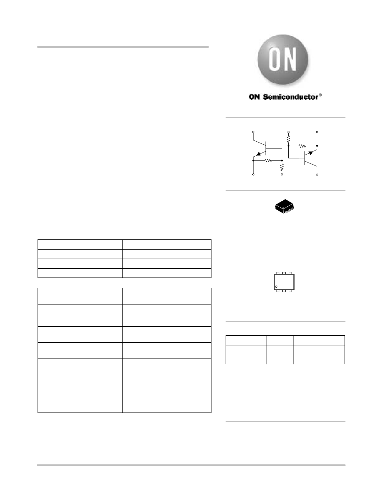
The BRT (Bias Resistor Transistor) contains a single transistor with
a monolithic bias network consisting of two resistors; a series base
resistor and a base−emitter resistor. These digital transistors are
designed to replace a single device and its external resistor bias
network. The BRT eliminates these individual components by
integrating them into a single device. In the NSB1011XV6T5, two
BRT devices are housed in the SOT−563 package which is ideal for
low power surface mount applications where board space is at a
premium.
• Simplifies Circuit Design
• Reduces Board Space
• Reduces Component Count
• This device is manufactured with a Pb−Free external lead finish only.
MAXIMUM RATINGS
(TA = 25°C unless otherwise noted, common for Q1 and Q2)
Rating
Collector-Base Voltage
Symbol
VCBO
Value
Unit
www.DataSheet4U.com
50 Vdc
Collector-Emitter Voltage
VCEO
50
Vdc
Collector Current
IC 100 mAdc
THERMAL CHARACTERISTICS
Characteristic
(One Junction Heated)
Symbol
Max
Unit
Total Device Dissipation
TA = 25°C
Derate above 25°C
PD
357 (Note 1)
mW
2.9 (Note 1) mW/°C
Thermal Resistance −
Junction-to-Ambient
RqJA
350 (Note 1)
°C/W
Characteristic
(Both Junctions Heated)
Symbol
Max
Unit
Total Device Dissipation
TA = 25°C
Derate above 25°C
PD
500 (Note 1)
mW
4.0 (Note 1) mW/°C
Thermal Resistance −
Junction-to-Ambient
RqJA
250 (Note 1)
°C/W
Junction and Storage
Temperature Range
TJ, Tstg −55 to +150
°C
Maximum ratings are those values beyond which device damage can occur.
Maximum ratings applied to the device are individual stress limit values (not
normal operating conditions) and are not valid simultaneously. If these limits are
exceeded, device functional operation is not implied, damage may occur and
reliability may be affected.
1. FR−4 @ Minimum Pad.
http://onsemi.com
(3) (2) (1)
R1 R2
Q1
R2 R1
Q2
(4) (5)
(6)
654
123
SOT−563
CASE 463A
PLASTIC
MARKING DIAGRAM
UT D
UT = Specific Device Code
(see table on following page)
D = Date Code
ORDERING INFORMATION
Device
Package
Shipping†
NSB1011XV6T5 SOT−563 8000 / Tape & Reel
(Pb−Free)
†For information on tape and reel specifications,
including part orientation and tape sizes, please
refer to our Tape and Reel Packaging Specifications
Brochure, BRD8011/D.
Preferred devices are recommended choices for future use
and best overall value.
Semiconductor Components Industries, LLC, 2005
January, 2005 − Rev. 0
1
Publication Order Number:
NSB1011XV6/D
1 page 
NSB1011XV6T5
A
−X−
654
12 3
G
PACKAGE DIMENSIONS
B
−Y−
D 65 PL
0.08 (0.003) M X Y
SOT−563, 6 LEAD
CASE 463A−01
ISSUE D
C
K
S
J
NOTES:
1. DIMENSIONING AND TOLERANCING PER
ANSI Y14.5M, 1982.
2. CONTROLLING DIMENSION: MILLIMETERS
3. MAXIMUM LEAD THICKNESS INCLUDES
LEAD FINISH THICKNESS. MINIMUM LEAD
THICKNESS IS THE MINIMUM THICKNESS
OF BASE MATERIAL.
MILLIMETERS INCHES
DIM MIN MAX MIN MAX
A 1.50 1.70 0.059 0.067
B 1.10 1.30 0.043 0.051
C 0.50 0.60 0.020 0.024
D 0.17 0.27 0.007 0.011
G 0.50 BSC
0.020 BSC
J 0.08 0.18 0.003 0.007
K 0.10 0.30 0.004 0.012
S 1.50 1.70 0.059 0.067
STYLE 1:
PIN 1. EMITTER 1
2. BASE 1
3. COLLECTOR 2
4. EMITTER 2
5. BASE 2
6. COLLECTOR 1
STYLE 2:
PIN 1. EMITTER 1
2. EMITTER2
3. BASE 2
4. COLLECTOR 2
5. BASE 1
6. COLLECTOR 1
STYLE 3:
PIN 1. CATHODE 1
2. CATHODE 1
3. ANODE/ANODE 2
4. CATHODE 2
5. CATHODE 2
6. ANODE/ANODE 1
STYLE 4:
PIN 1. COLLECTOR
2. COLLECTOR
3. BASE
4. EMITTER
5. COLLECTOR
6. COLLECTOR
SOLDERING FOOTPRINT*
0.3
0.0118
1.35
0.0531
1.0
0.0394
0.45
0.0177
0.5 0.5
0.0197 0.0197
ǒ ǓSCALE 20:1
mm
inches
*For additional information on our Pb−Free strategy and soldering
details, please download the ON Semiconductor Soldering and
Mounting Techniques Reference Manual, SOLDERRM/D.
http://onsemi.com
5
5 Page | ||
| Páginas | Total 6 Páginas | |
| PDF Descargar | [ Datasheet NSB1011XV6T5.PDF ] | |
Hoja de datos destacado
| Número de pieza | Descripción | Fabricantes |
| NSB1011XV6T5 | Dual Bias Resistor Transistors | ON Semiconductor |
| Número de pieza | Descripción | Fabricantes |
| SLA6805M | High Voltage 3 phase Motor Driver IC. |
Sanken |
| SDC1742 | 12- and 14-Bit Hybrid Synchro / Resolver-to-Digital Converters. |
Analog Devices |
|
DataSheet.es es una pagina web que funciona como un repositorio de manuales o hoja de datos de muchos de los productos más populares, |
| DataSheet.es | 2020 | Privacy Policy | Contacto | Buscar |