|
|
|
PDF ADC12C170 Data sheet ( Hoja de datos )
| Número de pieza | ADC12C170 | |
| Descripción | 12-Bit Bandwidth A/D Converter | |
| Fabricantes | National Semiconductor | |
| Logotipo | ||
Hay una vista previa y un enlace de descarga de ADC12C170 (archivo pdf) en la parte inferior de esta página. Total 22 Páginas | ||
|
No Preview Available !
February 2007
ADC12C170
12-Bit, 170 MSPS, 1.1 GHz Bandwidth A/D Converter with
CMOS outputs
General Description
Features
The ADC12C170 is a high-performance CMOS analog-to-
digital converter capable of converting analog input signals
into 12-Bit digital words at rates up to 170 Mega Samples Per
Second (MSPS). This converter uses a differential, pipelined
architecture with digital error correction and an on-chip sam-
ple-and-hold circuit to minimize power consumption and the
external component count, while providing excellent dynamic
performance. A unique sample-and-hold stage yields a full-
power bandwidth of 1.1 GHz. The ADC12C170 operates from
dual +3.3V and +1.8V power supplies and consumes 715 mW
of power at 170 MSPS.
■ 1.1 GHz Full Power Bandwidth
■ Internal sample-and-hold circuit
■ Low power consumption
■ Internal precision 1.0V reference
■ Single-ended or Differential clock modes
■ Clock Duty Cycle Stabilizer
■ Dual +3.3V and +1.8V supply operation (+/- 10%)
■ Power-down and Sleep modes
■ Offset binary or 2's complement output data format
The separate +1.8V supply for the digital output interface al- ■ Pin-compatible with: ADC14155
lows lower power operation with reduced noise. A power- ■ 48-pin LLP package, (7x7x0.8mm, 0.5mm pin-pitch)
down feature reduces the power consumption to 5 mW while
still allowing fast wake-up time to full operation. In addition
there is a sleep feature which consumes 50 mW of power and
has a faster wake-up time.
Key Specifications
■ Resolution
12 Bits
The differential inputs provide a full scale differential input
swing equal to 2 times the reference voltage. A stable 1.0V
■ Conversion Rate
■ SNR (fIN = 70 MHz)
170 MSPS
67.2 dBFS (typ)
internal voltage reference is provided, or the ADC12C170 can ■ SFDR (fIN = 70 MHz)
85.4 dBFS (typ)
be operated with an external reference.
Clock mode (differential versus single-ended)
and
output
dwawtwa.DataSh■■eet4EFU.ucNolmOl PBo(wfIeNr=B7a0ndMwHidzt)h
10.8 bits (typ)
1.1 GHz (typ)
format (offset binary versus 2's complement) are pin-se- ■ Power Consumption
715 mW (typ)
lectable. A duty cycle stabilizer maintains performance over
a wide range of input clock duty cycles.
Applications
The ADC12C170 is pin compatible with the ADC14155.
It is available in a 48-lead LLP package and operates over the
industrial temperature range of −40°C to +85°C.
■ High IF Sampling Receivers
■ Wireless Base Station Receivers
■ Power Amplifier Linearization
■ Multi-carrier, Multi-mode Receivers
■ Test and Measurement Equipment
■ Communications Instrumentation
■ Radar Systems
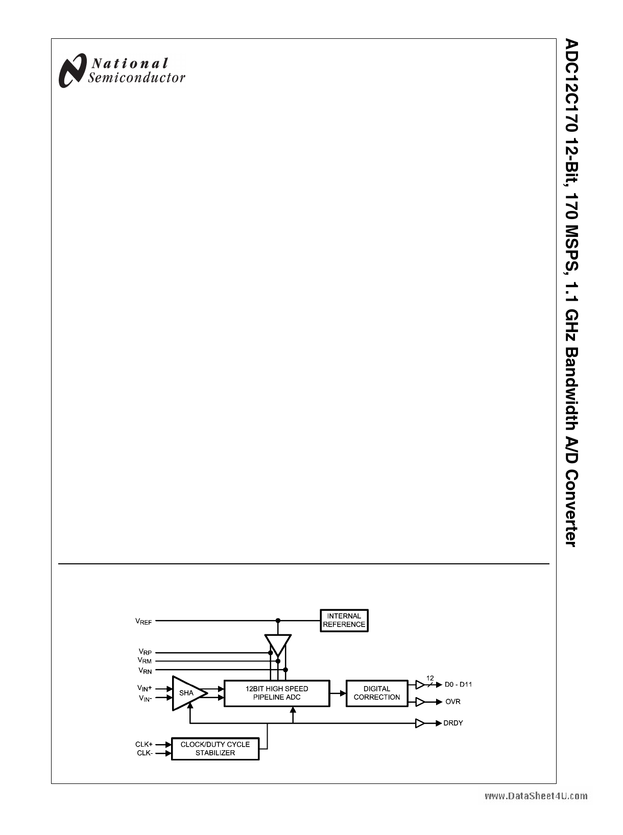
Block Diagram
© 2007 National Semiconductor Corporation 202092
20209202
www.national.com
1 page 
Absolute Maximum Ratings
(Notes 1, 2)
If Military/Aerospace specified devices are required,
please contact the National Semiconductor Sales Office/
Distributors for availability and specifications.
Supply Voltage (VA, VD)
Supply Voltage (VDR)
|VA–VD|
−0.3V to 4.2V
−0.3V to 2.35V
≤ 100 mV
Voltage on Any Input Pin
(Not to exceed 4.2V)
−0.3V to (VA +0.3V)
Voltage on Any Output Pin
(Not to exceed 2.35V)
-0.3V to (VDR +0.2V)
Input Current at Any Pin other
than Supply Pins (Note 3)
±5 mA
Package Input Current (Note 3)
±50 mA
Max Junction Temp (TJ)
Thermal Resistance (θJA)
Package Dissipation at TA = 25°
C (Note 4)
+150°C
24°C/W
5.2W
ESD Rating
Human Body Model (Note 5)
2000 V
Machine Model (Note 5)
200 V
Charge Device Model
1000 V
Storage Temperature
−65°C to +150°C
Soldering process must comply with National
Semiconductor's Reflow Temperature Profile
specifications. Refer to www.national.com/packaging.
(Note 6)
Operating Ratings (Notes 1, 2)
Operating Temperature
Supply Voltage (VA, VD)
Output Driver Supply (VDR)
CLK
Clock Duty Cycle
Analog Input Pins
VCM
|AGND-DGND|
−40°C ≤ TA ≤ +85°C
+3.0V to +3.6V
+1.6V to +2.0V
−0.05V to (VA + 0.05V)
30/70 %
0V to 2.6V
1.4V to 1.6V
≤100mV
www.DataSheet4U.com
5 www.national.com
5 Page 
Timing Diagram
Transfer Characteristic
Output Timing
www.DataSheet4U.com
20209209
FIGURE 1. Transfer Characteristic (Offset Binary Format)
11
20209210
www.national.com
11 Page | ||
| Páginas | Total 22 Páginas | |
| PDF Descargar | [ Datasheet ADC12C170.PDF ] | |
Hoja de datos destacado
| Número de pieza | Descripción | Fabricantes |
| ADC12C170 | 12-Bit Bandwidth A/D Converter | National Semiconductor |
| ADC12C170 | ADC12C170 12-Bit 170 MSPS 1.1 GHz Bandwidth A/D Converter with CMOS Outputs (Rev. E) | Texas Instruments |
| Número de pieza | Descripción | Fabricantes |
| SLA6805M | High Voltage 3 phase Motor Driver IC. |
Sanken |
| SDC1742 | 12- and 14-Bit Hybrid Synchro / Resolver-to-Digital Converters. |
Analog Devices |
|
DataSheet.es es una pagina web que funciona como un repositorio de manuales o hoja de datos de muchos de los productos más populares, |
| DataSheet.es | 2020 | Privacy Policy | Contacto | Buscar |